DC-VIDEO-TVP5146N Altera, DC-VIDEO-TVP5146N Datasheet - Page 20
DC-VIDEO-TVP5146N
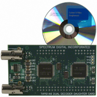
Manufacturer Part Number
DC-VIDEO-TVP5146N
Description
VIDEO DAUGHTER CARD
Manufacturer
Altera
Series
Stratix® IIIr
Datasheets
1.EP3SL150F780C4N.pdf
(16 pages)
2.EP3SL150F780C4N.pdf
(332 pages)
3.DC-VIDEO-TVP5146N.pdf
(58 pages)
Specifications of DC-VIDEO-TVP5146N
Main Purpose
Video, Daughter Card
Embedded
No
Utilized Ic / Part
Altera Dev Kits
Primary Attributes
Dual Composite Video Input - NTSC or PAL
Secondary Attributes
10-bit BT.656 Output, Compatible with Expansion Connector, Standard on Most Altera Development Kits
Lead Free Status / RoHS Status
Lead free / RoHS Compliant
Other names
544-1704


1–20
Table 1–22. TriMatrix Memory Block Performance Specifications for Stratix III Devices
Stratix III Device Handbook, Volume 2
M144K
(3),
Notes to
(1) Use a memory block clock that comes through global clock routing from an on-chip PLL set to 50% output duty cycle to achieve the maximum memory block
(2) The F
(3) The F
(4) F
(5) F
(6) The F
Memory
Block
Type
(5)
performance. Use the Quartus II software to report timing for this and other memory block clocking schemes.
C4L speed grade with V
max
max
Table
is applicable when the COMPTABILITY option is turned ON.
is applicable when the COMPTABILITY option is turned OFF. This option is turned ON by default in Quartus II software.
max
max
max
Simple dual-port 2K × 64 (with ECC)
Min Pulse Width (Clock High Time)
Min Pulse Width (Clock Low Time)
shown for M9K degrades 2% when you use the Error Detection CRC feature on the device, except for the C4L speed grade with V
shown for M144K degrades 10 MHz when you use byte-enable support on M144K.
for the EP3SL200, EP3SE260, and EP3SL340 devices at the C2 speed grade is 7% slower than the C2 values shown in the table.
1–22:
Configuration and JTAG Specifications
Table 1–23
Table 1–23. Configuration Mode Specifications for Stratix III Devices
Table 1–24
the figure for “HIGH-SPEED I/O Block” in the
JTAG timing requirements.
Table 1–24. JTAG Timing Parameters and Values for Stratix III Devices
Passive Serial
Fast Passive Parallel
Fast Active Serial
Notes to
(1) DCLK F
(2) The data rate must be 4× slower than the clock when you use decompression and/or encryption.
(3) For more information about the minimum and typical DCLK F
t
t
t
t
t
t
t
t
t
CCL
Mode
JCP
JCH
JCL
JPSU
JPSU
JPH
JPCO
JPZX
JPXZ
= 0.9V, there is no degradation in F
Symbol
Update Circuitry (ALTREMOTE_UPDATE) Megafunction User
the
(TDI)
(TMS)
Configuring Stratix III Devices
Table
max
lists the JTAG timing parameters and values for Stratix III devices. Refer to
lists the Stratix III configuration mode specifications.
is restricted when you enable the Remote Update feature. For more information, refer to the
1–23:
TCK clock period
TCK clock high time
TCK clock low time
JTAG port setup time for TDI
JTAG port setup time for TMS
JTAG port hold time
JTAG port clock to output
JTAG port high impedance to valid output
JTAG port valid output to high impedance
(3)
Programming Mode
(2)
ALUTs
—
—
0
TriMatrix
Memory
Parameter
max
chapter.
—
—
1
when you use the Error Detection CRC feature.
Chapter 1: Stratix III Device Datasheet: DC and Switching Characteristics
C2
1.1 V
V
255
800
500
CCL
(6)
=
V
1.1 V
1000
210
625
C3
CCL
“Glossary” on page 1–326
=
max
Guide.
value in Fast Active Serial configuration, refer to
V
1.1 V
1100
180
690
C4
CCL
(Note 1)
=
Min
30
14
14
—
—
—
1
3
5
DCLK F
V
1.1 V
1100
180
690
100
100
CCL
40
(Note 1)
=
C4L
© July 2010 Altera Corporation
max
(Part 3 of 3)
0.9 V
V
1800
1100
130
CCL
Max
—
—
—
—
—
—
11
14
14
Switching Characteristics
=
1.1 V
V
1000
195
625
I3
CCL
for the
=
MHz
MHz
MHz
Unit
Unit
1.1 V
Remote
V
1100
ns
ns
ns
ns
ns
ns
ns
ns
ns
180
690
I4
CCL
=
CCL
= 0.9 V. For the
0.9 V
V
1800
1100
I4L
120
CCL
=
Unit
MHz
ps
ps
Related parts for DC-VIDEO-TVP5146N
Image
Part Number
Description
Manufacturer
Datasheet
Request
R

Part Number:
Description:
CYCLONE II STARTER KIT EP2C20N
Manufacturer:
Altera
Datasheet:


Part Number:
Description:
CPLD, EP610 Family, ECMOS Process, 300 Gates, 16 Macro Cells, 16 Reg., 16 User I/Os, 5V Supply, 35 Speed Grade, 24DIP
Manufacturer:
Altera Corporation
Datasheet:
Part Number:
Description:
CPLD, EP610 Family, ECMOS Process, 300 Gates, 16 Macro Cells, 16 Reg., 16 User I/Os, 5V Supply, 15 Speed Grade, 24DIP
Manufacturer:
Altera Corporation
Datasheet:
Part Number:
Description:
Manufacturer:
Altera Corporation
Datasheet:
Part Number:
Description:
CPLD, EP610 Family, ECMOS Process, 300 Gates, 16 Macro Cells, 16 Reg., 16 User I/Os, 5V Supply, 30 Speed Grade, 24DIP
Manufacturer:
Altera Corporation
Datasheet:
Part Number:
Description:
High-performance, low-power erasable programmable logic devices with 8 macrocells, 10ns
Manufacturer:
Altera Corporation
Datasheet:
Part Number:
Description:
High-performance, low-power erasable programmable logic devices with 8 macrocells, 7ns
Manufacturer:
Altera Corporation
Datasheet:
Part Number:
Description:
Classic EPLD
Manufacturer:
Altera Corporation
Datasheet:
Part Number:
Description:
High-performance, low-power erasable programmable logic devices with 8 macrocells, 10ns
Manufacturer:
Altera Corporation
Datasheet:
Part Number:
Description:
Manufacturer:
Altera Corporation
Datasheet:
Part Number:
Description:
Manufacturer:
Altera Corporation
Datasheet:
Part Number:
Description:
Manufacturer:
Altera Corporation
Datasheet:
Part Number:
Description:
CPLD, EP610 Family, ECMOS Process, 300 Gates, 16 Macro Cells, 16 Reg., 16 User I/Os, 5V Supply, 25 Speed Grade, 24DIP
Manufacturer:
Altera Corporation
Datasheet: