C8051F700-TB Silicon Laboratories Inc, C8051F700-TB Datasheet - Page 86
C8051F700-TB
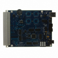
Manufacturer Part Number
C8051F700-TB
Description
BOARD PROTOTYPE WITH C8051F700
Manufacturer
Silicon Laboratories Inc
Datasheets
1.C8051F700-TB.pdf
(1 pages)
2.C8051F700-TB.pdf
(306 pages)
3.C8051F700-TB.pdf
(18 pages)
Specifications of C8051F700-TB
Accessory Type
Target Board
Processor To Be Evaluated
C8051F700
Processor Series
C8051F7xx
Interface Type
USB
Operating Supply Voltage
7 V to 15 V
Lead Free Status / RoHS Status
Lead free / RoHS Compliant
For Use With/related Products
C8051F7xx
Lead Free Status / Rohs Status
Lead free / RoHS Compliant
Other names
336-1637
C8051F700
C8051F700


C8051F70x/71x
15.7. CS0 Pin Monitor
The CS0 module provides accurate conversions in all operating modes of the CPU, peripherals and I/O
ports. Pin monitoring circuits are provided to improve interference immunity from high-current output pin
switching. The Capacitive Sense Pin Monitor register (CS0PM, SFR Definition 15.9) controls the operation
of these pin monitors.
Conversions in the CS0 module are immune to any change on digital inputs and immune to most output
switching. Even high-speed serial data transmission will not affect CS0 operation as long as the output
load is limited. Output changes that switch large loads such as LEDs and heavily-loaded communications
lines can affect conversion accuracy. For this reason, the CS0 module includes pin monitoring circuits that
will, if enabled, automatically adjust conversion timing if necessary to eliminate any effect from high-current
output pin switching.
The pin monitor enable bit should be set for any output signal that is expected to drive a large load.
Example: The SMBus in a system is heavily loaded with multiple slaves and a long PCB route. Set the
SMBus pin monitor enable, SMBPM = 1.
Example: Timer2 controls an LED on Port 1, pin 3 to provide variable dimming. Set the Port SFR write
monitor enable, PIOPM = 1.
Example: The SPI bus is used to communicate to a nearby host. The pin monitor is not needed because
the output is not heavily loaded, SPIPM remains = 0, the default reset state.
Pin monitors should not be enabled unless they are required. The pin monitor works by repeating any por-
tion of a conversion that may have been corrupted by a change on an output pin. Setting pin monitor
enables bits will slow CS0 conversions.
The frequency of CS0 retry operations can be limited by setting the CSPMMD bits. In the default (reset)
state, all converter retry requests will be performed. This is the recommended setting for all applications.
The number of retries per conversion can be limited to either two or four retries by changing CSPMMD.
Limiting the number of retries per conversion ensures that even in circumstances where extremely fre-
quent high-power output switching occurs, conversions will be completed, though there may be some loss
of accuracy due to switching noise.
Activity of the pin monitor circuit can be detected by reading the Pin Monitor Event bit, CS0PME, in register
CS0CN. This bit will be set if any CS0 converter retries have occurred. It remains set until cleared by soft-
ware or a device reset.
86
Rev. 1.0
Related parts for C8051F700-TB
Image
Part Number
Description
Manufacturer
Datasheet
Request
R

Part Number:
Description:
SMD/C°/SINGLE-ENDED OUTPUT SILICON OSCILLATOR
Manufacturer:
Silicon Laboratories Inc
Part Number:
Description:
Manufacturer:
Silicon Laboratories Inc
Datasheet:
Part Number:
Description:
N/A N/A/SI4010 AES KEYFOB DEMO WITH LCD RX
Manufacturer:
Silicon Laboratories Inc
Datasheet:
Part Number:
Description:
N/A N/A/SI4010 SIMPLIFIED KEY FOB DEMO WITH LED RX
Manufacturer:
Silicon Laboratories Inc
Datasheet:
Part Number:
Description:
N/A/-40 TO 85 OC/EZLINK MODULE; F930/4432 HIGH BAND (REV E/B1)
Manufacturer:
Silicon Laboratories Inc
Part Number:
Description:
EZLink Module; F930/4432 Low Band (rev e/B1)
Manufacturer:
Silicon Laboratories Inc
Part Number:
Description:
I°/4460 10 DBM RADIO TEST CARD 434 MHZ
Manufacturer:
Silicon Laboratories Inc
Part Number:
Description:
I°/4461 14 DBM RADIO TEST CARD 868 MHZ
Manufacturer:
Silicon Laboratories Inc
Part Number:
Description:
I°/4463 20 DBM RFSWITCH RADIO TEST CARD 460 MHZ
Manufacturer:
Silicon Laboratories Inc
Part Number:
Description:
I°/4463 20 DBM RADIO TEST CARD 868 MHZ
Manufacturer:
Silicon Laboratories Inc
Part Number:
Description:
I°/4463 27 DBM RADIO TEST CARD 868 MHZ
Manufacturer:
Silicon Laboratories Inc
Part Number:
Description:
I°/4463 SKYWORKS 30 DBM RADIO TEST CARD 915 MHZ
Manufacturer:
Silicon Laboratories Inc
Part Number:
Description:
N/A N/A/-40 TO 85 OC/4463 RFMD 30 DBM RADIO TEST CARD 915 MHZ
Manufacturer:
Silicon Laboratories Inc
Part Number:
Description:
I°/4463 20 DBM RADIO TEST CARD 169 MHZ
Manufacturer:
Silicon Laboratories Inc