C8051F700-TB Silicon Laboratories Inc, C8051F700-TB Datasheet - Page 65
C8051F700-TB
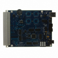
Manufacturer Part Number
C8051F700-TB
Description
BOARD PROTOTYPE WITH C8051F700
Manufacturer
Silicon Laboratories Inc
Datasheets
1.C8051F700-TB.pdf
(1 pages)
2.C8051F700-TB.pdf
(306 pages)
3.C8051F700-TB.pdf
(18 pages)
Specifications of C8051F700-TB
Accessory Type
Target Board
Processor To Be Evaluated
C8051F700
Processor Series
C8051F7xx
Interface Type
USB
Operating Supply Voltage
7 V to 15 V
Lead Free Status / RoHS Status
Lead free / RoHS Compliant
For Use With/related Products
C8051F7xx
Lead Free Status / Rohs Status
Lead free / RoHS Compliant
Other names
336-1637
C8051F700
C8051F700


10.5. ADC0 Analog Multiplexer
ADC0 on the C8051F700/2/4/6/8 and C8051F710/2/4/6 uses an analog input multiplexer to select the pos-
itive input to the ADC. Any of the following may be selected as the positive input: Port 0 or Port 1 I/O pins,
the on-chip temperature sensor, or the positive power supply (V
the ADC0MX register described in SFR Definition 10.9.
Important Note About ADC0 Input Configuration: Port pins selected as ADC0 inputs should be config-
ured as analog inputs, and should be skipped by the Digital Crossbar. To configure a Port pin for analog
input, set the corresponding bit in register PnMDIN to 0. To force the Crossbar to skip a Port pin, set the
corresponding bit in register PnSKIP to 1. See Section “28. Port Input/Output” on page 180 for more Port
I/O configuration details.
Sensor
Temp
VREG Output
Figure 10.6. ADC0 Multiplexer Block Diagram
P0.0
P1.7
GND
VDD
ADC0MX
Rev. 1.0
AMUX
DD
). The ADC0 input channel is selected in
C8051F70x/71x
ADC0
65
Related parts for C8051F700-TB
Image
Part Number
Description
Manufacturer
Datasheet
Request
R

Part Number:
Description:
SMD/C°/SINGLE-ENDED OUTPUT SILICON OSCILLATOR
Manufacturer:
Silicon Laboratories Inc
Part Number:
Description:
Manufacturer:
Silicon Laboratories Inc
Datasheet:
Part Number:
Description:
N/A N/A/SI4010 AES KEYFOB DEMO WITH LCD RX
Manufacturer:
Silicon Laboratories Inc
Datasheet:
Part Number:
Description:
N/A N/A/SI4010 SIMPLIFIED KEY FOB DEMO WITH LED RX
Manufacturer:
Silicon Laboratories Inc
Datasheet:
Part Number:
Description:
N/A/-40 TO 85 OC/EZLINK MODULE; F930/4432 HIGH BAND (REV E/B1)
Manufacturer:
Silicon Laboratories Inc
Part Number:
Description:
EZLink Module; F930/4432 Low Band (rev e/B1)
Manufacturer:
Silicon Laboratories Inc
Part Number:
Description:
I°/4460 10 DBM RADIO TEST CARD 434 MHZ
Manufacturer:
Silicon Laboratories Inc
Part Number:
Description:
I°/4461 14 DBM RADIO TEST CARD 868 MHZ
Manufacturer:
Silicon Laboratories Inc
Part Number:
Description:
I°/4463 20 DBM RFSWITCH RADIO TEST CARD 460 MHZ
Manufacturer:
Silicon Laboratories Inc
Part Number:
Description:
I°/4463 20 DBM RADIO TEST CARD 868 MHZ
Manufacturer:
Silicon Laboratories Inc
Part Number:
Description:
I°/4463 27 DBM RADIO TEST CARD 868 MHZ
Manufacturer:
Silicon Laboratories Inc
Part Number:
Description:
I°/4463 SKYWORKS 30 DBM RADIO TEST CARD 915 MHZ
Manufacturer:
Silicon Laboratories Inc
Part Number:
Description:
N/A N/A/-40 TO 85 OC/4463 RFMD 30 DBM RADIO TEST CARD 915 MHZ
Manufacturer:
Silicon Laboratories Inc
Part Number:
Description:
I°/4463 20 DBM RADIO TEST CARD 169 MHZ
Manufacturer:
Silicon Laboratories Inc