130-28176 Parallax Inc, 130-28176 Datasheet - Page 73
130-28176
Manufacturer Part Number
130-28176
Description
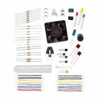
KIT PARTS PROCESS CONTROL
Manufacturer
Parallax Inc
Specifications of 130-28176
Accessory Type
Education Kit
Product
Microcontroller Accessories
Lead Free Status / RoHS Status
Contains lead / RoHS non-compliant
For Use With/related Products
Board of Education Full Kit
Lead Free Status / RoHS Status
Lead free / RoHS Compliant, Contains lead / RoHS non-compliant


Voltage and Current Characteristics
Cutoff Region:
With insufficient base current, the transistor will essentially be off (an open switch) and
acts as a very high resistance from collector to emitter. I
the output (V
V
Linear Region:
In the linear region, the collector current, (I
by the DC gain of the transistor, h
a
For example, given: h
What if I
Does this make sense? How did we get 20 V across R
transistor had long gone into saturation when V
applied across R
CUTOFF
function
.
I
V
V
I
V
V
B
C
C
RC
CE
RC
CE
Vcc vs. Vdd Officially, the collector voltage is called Vcc when working with BJTs which
have a collector. Vdd is more properly used with Field Effect Transistors (FET) which have
a drain instead of a collector. The BASIC Stamp is constructed with FETs, thus the Vdd
designation is used.
were 100 µA? What do the calculations show for I
= I
= I
= Vdd −V
= Vdd −V
= I
= I
B
B
CE
of
h
h
C
C
) will be supply voltage, or Vdd in this case. This is also known as
C
FE
FE
.
R
R
= (10 µA)(200) = 2000 µA = 2 mA.
C
C
= (100 µA)(200) = 20000 µA = 20 mA.
the
= (2 mA)(1 kΩ) = 2 V
= (20 mA)(1 kΩ) = 20 V
FE
RC
RC
= 200, I
= 5 V−2 V = 3 V
= 5 V − 20 V = −15 V
current
B
=10 µA, and a 5 V supply; calculate I
FE
. The 2N3904 can have a gain of 100 to 300. V
flow,
C
creating
), is a function of the base-current multiplied
CE
went down to 0 V and all of Vdd was
a
C
C
will be zero, and the voltage at
voltage
with a supply of 5 V? The
C
, V
RC
and V
drop
C
, V
CE
RC
?
across
and V
CE
CE
.
R
is
C
.
Related parts for 130-28176
Image
Part Number
Description
Manufacturer
Datasheet
Request
R

Part Number:
Description:
KIT PROPELLER EDU PROJECT PARTS
Manufacturer:
Parallax Inc
Datasheet:

Part Number:
Description:
KIT PARTS SMART SENSORS
Manufacturer:
Parallax Inc
Datasheet:


Part Number:
Description:
Microcontroller Modules & Accessories DISCONTINUED BY PARALLAX
Manufacturer:
Parallax Inc

Part Number:
Description:
BOOK UNDERSTANDING SIGNALS
Manufacturer:
Parallax Inc
Datasheet:


Part Number:
Description:
COMPETITION RING FOR SUMOBOT
Manufacturer:
Parallax Inc
Datasheet:


Part Number:
Description:
TEXT INFRARED REMOTE FOR BOE-BOT
Manufacturer:
Parallax Inc
Datasheet:
Part Number:
Description:
Microcontroller Modules & Accessories DISCONTINUED BY PARALLAX
Manufacturer:
Parallax Inc
Part Number:
Description:
BOOK UNDERSTANDING SIGNALS
Manufacturer:
Parallax Inc
Datasheet:
Part Number:
Description:
BOARD EXPERIMENT+LCD NX-1000
Manufacturer:
Parallax Inc
Datasheet:
Part Number:
Description:
IC MCU 2K FLASH 50MHZ SO-18
Manufacturer:
Parallax Inc
Datasheet: