130-28176 Parallax Inc, 130-28176 Datasheet - Page 172
130-28176
Manufacturer Part Number
130-28176
Description
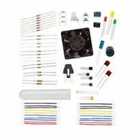
KIT PARTS PROCESS CONTROL
Manufacturer
Parallax Inc
Specifications of 130-28176
Accessory Type
Education Kit
Product
Microcontroller Accessories
Lead Free Status / RoHS Status
Contains lead / RoHS non-compliant
For Use With/related Products
Board of Education Full Kit
Lead Free Status / RoHS Status
Lead free / RoHS Compliant, Contains lead / RoHS non-compliant


You may note the voltage increasing slightly over time. Very small leakage through the
non-inverting input is causing the capacitor to charge further. While not critical, if not
refreshed regularly (occurs when StampPlot is not connected), the voltage at the output
will rise to maximum over several minutes.
What occurs as the PWM is adjusted to maximum? Do you still get 5 V out? Chances
are, you see a maximum voltage around 3.5 V. The output of the op-amp cannot be
higher than the voltage supplied to it, and, in fact, will be 1 to 2 volts less than the rail or
supply voltages. To overcome this problem, the op-amp can be supplied from a higher
voltage – Vin on our boards.
Another name for the combination of filter and op-amp buffer is an active low-pass filter.
If we could adjust the input frequency, the maximum frequency (cutoff frequency)
allowed to be passed before being dramatically attenuated is 1/(2πRC).
In our example, attenuation is good because it is being filtered to a DC level leaving no
ripple or AC component. The PWM at 112 kHz is well above the cutoff frequency.
A high-pass filter, or one that blocks low frequencies while allowing high frequencies to
pass, has the resistor and capacitor positions in the circuit reversed but uses the same
formula for cutoff frequency.
ACTIVITY #5: OP-AMP NON-INVERTING AMPLIFIER
The buffer has a gain of 1, or unity gain. For each 1 V change in the input, there is a 1 V
change in the output. With an input of V
balance the inverting and non-inverting inputs.
√
√
√
Adjust the drive, which should produce stable voltages.
Connect pin 8 of the op-amp (NOT P8 on the BASIC Stamp!) to Vin. Ensure
this voltage is not connected to any other devices that may be damaged by it.
Retest the maximum voltage achieved.
f
CUTOFF
= 1/(2πRC) = 1/(2 x 3.14 x 10 kΩ x 0.68 µF) = 23.4 Hz
I
= 2 V, the output has to drive at V
O
= 2 V to
Related parts for 130-28176
Image
Part Number
Description
Manufacturer
Datasheet
Request
R

Part Number:
Description:
KIT PROPELLER EDU PROJECT PARTS
Manufacturer:
Parallax Inc
Datasheet:

Part Number:
Description:
KIT PARTS SMART SENSORS
Manufacturer:
Parallax Inc
Datasheet:


Part Number:
Description:
Microcontroller Modules & Accessories DISCONTINUED BY PARALLAX
Manufacturer:
Parallax Inc

Part Number:
Description:
BOOK UNDERSTANDING SIGNALS
Manufacturer:
Parallax Inc
Datasheet:


Part Number:
Description:
COMPETITION RING FOR SUMOBOT
Manufacturer:
Parallax Inc
Datasheet:


Part Number:
Description:
TEXT INFRARED REMOTE FOR BOE-BOT
Manufacturer:
Parallax Inc
Datasheet:
Part Number:
Description:
Microcontroller Modules & Accessories DISCONTINUED BY PARALLAX
Manufacturer:
Parallax Inc
Part Number:
Description:
BOOK UNDERSTANDING SIGNALS
Manufacturer:
Parallax Inc
Datasheet:
Part Number:
Description:
BOARD EXPERIMENT+LCD NX-1000
Manufacturer:
Parallax Inc
Datasheet:
Part Number:
Description:
IC MCU 2K FLASH 50MHZ SO-18
Manufacturer:
Parallax Inc
Datasheet: