HSC-ADC-EVALCZ Analog Devices Inc, HSC-ADC-EVALCZ Datasheet - Page 23
HSC-ADC-EVALCZ
Manufacturer Part Number
HSC-ADC-EVALCZ
Description
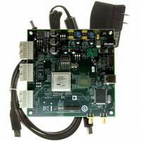
KIT EVAL ADC FIFO HI SPEED
Manufacturer
Analog Devices Inc
Datasheets
1.HSC-ADC-EVALB-DCZ.pdf
(28 pages)
2.HSC-ADC-EVALCZ.pdf
(32 pages)
3.HSC-ADC-EVALCZ.pdf
(40 pages)
Specifications of HSC-ADC-EVALCZ
Design Resources
EVALC PC Board Gerber File
Accessory Type
ADC Interface Board
Silicon Manufacturer
Analog Devices
Application Sub Type
ADC
Kit Application Type
Data Converter
Features
Buffer Memory Board For Capturing Digital Data, USB Port Interface, Windows 98, Windows 2000
Kit Contents
ADC Analyzer, Buffer Memory Board
Rohs Compliant
Yes
Lead Free Status / RoHS Status
Lead free / RoHS Compliant
For Use With/related Products
Single ADC Version
Lead Free Status / Rohs Status
Supplier Unconfirmed
Available stocks
Company
Part Number
Manufacturer
Quantity
Price
Company:

Part Number:
HSC-ADC-EVALCZ
Manufacturer:
Analog Devices Inc
Quantity:
135


COMPONENTS MODELS
In many instances, it may be desirable to use behavioral models
instead of real devices, such as when test hardware is not avail-
able or if a device is in preselection phase. No matter the case,
VisualAnalog supports converter models in addition to physical
hardware, enabling a virtual test bench. Currently only ADC
models are available using the Analog Devices ADIsimADC™
platform. This provides a seamless integration of models into
the evaluation platform. It is also possible to include both
models and real devices at the same time to compare predicted
vs. actual performance.
ADC MODEL
The ADC Model component interfaces with ADIsimADC
to simulate ADC performance. The model interface provides
translation from the analog domain to the digital domain. To
access ADC Model Settings click Settings.
Figure 48. ADC Model and Settings Form
Rev. 0 | Page 23 of 40
The model interface allows selection of the desired model,
setting of the analog input range (the actual analog frequency
is detected or may be overridden by selecting the Nyquist zone),
and setting any external clock jitter—the default is that used
during characterization by Analog Devices. Internal device jitter
is automatically included and cannot be changed. More infor
mation about ADIsimADC is available at
www.analog.com/adisimadc.
When using the ADC Model component, the two input termi
nals on the left represent the input waveform on the top and a
tone list on the bottom. When connecting to a VisualAnalog
Tone Generator (see the Tone Generator section). the input
terminals of the ADIsimADC™ model map directly to the
output terminals of the Tone Generator. The ADC Model
component uses the tone list input to set the spectral center
frequency. When connecting the input to other components,
you can leave the lower input disconnected, and enter the
spectral center manually.
An Input Formatter must always follow the ADC Model
Component if you want to pedrform processing within the
canvas. The only exception to this rule is Logic Analysis. The
Input Formatter takes the resolution of the ADC into account
when moving data into the environment of VisualAnalog. For
more information on setting up the Input Formatter, see the
Input Formatter section.
All Analog Devices models are LSB-justified and, therefore,
the Alignment check box within the Input Formatter should
be set to the native resolution of the model. The resolution on
the Input Formatter should be set to the native resolution of
the model as well. Note that the alignment setting is different
when using the Input Formatter with the ADC Data Capture
component. The number format should be set in accordance
with the data format of the ADC model.
AN-905
Related parts for HSC-ADC-EVALCZ
Image
Part Number
Description
Manufacturer
Datasheet
Request
R

Part Number:
Description:
KIT EVAL ADC FIFO DUAL-CH USB HS
Manufacturer:
Analog Devices Inc
Datasheet:

Part Number:
Description:
KIT EVAL ADC USB FIFO HI-SPEED
Manufacturer:
Analog Devices Inc
Datasheet:

Part Number:
Description:
BOARD FPGA OCTAL LVDS FOR ADC
Manufacturer:
Analog Devices Inc
Datasheet:
Part Number:
Description:
KIT EVAL FOR SINGLE CHAN HSC ADC
Manufacturer:
Analog Devices Inc

Part Number:
Description:
KIT EVAL FOR DUAL ADC/CONV
Manufacturer:
Analog Devices Inc
Datasheet:
Part Number:
Description:
KIT EVAL ADC USB FIFO HI-SPEED
Manufacturer:
Analog Devices Inc
Datasheet:

Part Number:
Description:
KIT EVAL ADC USB FIFO HI-SPEED
Manufacturer:
Analog Devices Inc
Datasheet:
Part Number:
Description:
KIT EVAL ADC FIFO DUAL-CH USB HS
Manufacturer:
Analog Devices Inc
Datasheet:
Part Number:
Description:
BOARD FPGA QUAD LVDS FOR ADC
Manufacturer:
Analog Devices Inc
Datasheet:
Part Number:
Description:
Adapter For AD922x Family
Manufacturer:
Analog Devices Inc
Datasheet:
Part Number:
Description:
Interposer Quad/octal ADCs
Manufacturer:
Analog Devices Inc
Datasheet:

Part Number:
Description:
±1.7g Dual-Axis IMEMS Accelerometer Evaluation Board
Manufacturer:
Analog Devices Inc
Datasheet:

Part Number:
Description:
IC MULTIPLIER ANALOG 8-SOIC T/R
Manufacturer:
Analog Devices Inc
Datasheet:
Part Number:
Description:
IC ANALOG MULTIPLIER 8-DIP
Manufacturer:
Analog Devices Inc
Datasheet: