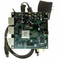
HSC-ADC-EVALCZ Analog Devices Inc, HSC-ADC-EVALCZ Datasheet - Page 19
HSC-ADC-EVALCZ
Manufacturer Part Number
HSC-ADC-EVALCZ
Description
KIT EVAL ADC FIFO HI SPEED
Manufacturer
Analog Devices Inc
Datasheets
1.HSC-ADC-EVALB-DCZ.pdf
(28 pages)
2.HSC-ADC-EVALCZ.pdf
(32 pages)
3.HSC-ADC-EVALCZ.pdf
(40 pages)
Specifications of HSC-ADC-EVALCZ
Design Resources
EVALC PC Board Gerber File
Accessory Type
ADC Interface Board
Silicon Manufacturer
Analog Devices
Application Sub Type
ADC
Kit Application Type
Data Converter
Features
Buffer Memory Board For Capturing Digital Data, USB Port Interface, Windows 98, Windows 2000
Kit Contents
ADC Analyzer, Buffer Memory Board
Rohs Compliant
Yes
Lead Free Status / RoHS Status
Lead free / RoHS Compliant
For Use With/related Products
Single ADC Version
Lead Free Status / Rohs Status
Supplier Unconfirmed
Available stocks
Company
Part Number
Manufacturer
Quantity
Price
Company:

Part Number:
HSC-ADC-EVALCZ
Manufacturer:
Analog Devices Inc
Quantity:
135


ADC DATA CAPTURE
The ADC Data Capture component is responsible for
acquiring data from high speed ADC data capture boards.
This component interfaces with a wide variety of ADCs,
including those with specialty outputs such as power and
other on-chip measurements.
An Input Formatter must always follow the ADC Data
Capture component if you want to perform processing within
the canvas. The only exception to this rule is Logic Analysis.
The Input Formatter takes the resolution and alignment of the
ADC into account when moving data into the environment of
VisualAnalog. For more information on setting up the Input
Formatter, see the Input Formatter section.
Most of the Analog Devices ADC evaluation boards are MSB-
justified to 16 bits and, therefore, the Alignment box within the
Input Formatter should be set to 16 bits. The resolution on the
Input Formatter should be set to the native resolution of the
ADC. Number Format should be set in accordance with the
data format of the ADC.
Access ADC Data Capture Settings by clicking Settings.
Use the General tab to set parameters about the device you are
using and the data you want to capture.
Capture—Shows the USB devices available. Use this drop-down
box to select the board you want to use. Boards appear in the
order in which they were connected. If no devices are found,
check the cables and power supplies and click Refresh.
ADC—Displays special configurations available for the ADC
that you are using. Select one or use the Default setting.
Clock Frequency (MHz) —Should be set to the sample rate of
the device.
Figure 40. ADC Data Capture and Settings Form, General Tab
Rev. 0 | Page 19 of 40
Output Data—Determines which outputs the component
passes back to the canvas. You can choose multiple outputs that
provide data from multiple core ADC outputs or pass the same
output to multiple processes on the canvas much like the Data
Router component. Modify the default options for Output
Data with the Add, Remove or Clear buttons. To add a new
selection, simply choose from the available selections in the
Select Data drop-down box and click Add. Remove deletes an
existing Output Data entry. Clear removes all outputs and
allows a completely new set of outputs to be added.
In Output Data, set the length to the sample size of the capture
board FIFO or the desired sample size, whichever is less.
Normally, the HSC-ADC-EVALA and HSC-ADC-EVALB
boards have 32-KB devices. It is possible to reconfigure them
with compatible 256-KB devices. The HSC-ADC-EVALC board
can support various sample sizes, depending on the current
FPGA configuration.
Use the Board Settings tab to set board-related parameters.
FIFO Fill allows you to adjust parameters that are used while
filling the on-board FIFOs with ADC data. Normally, the soft
ware sends the fill command to the FIFOs and waits a specified
amount of time before reading the data. You can set the delay
time by inserting the desired amount in the Fill Delay (ms)
option.
When you have a slow clock rate, sometimes it is useful to
poll the FIFOs for a full flag, which indicates when the FIFOs
are full. Select the Poll Full Flag check box and then set the
Maximum Poll Time so the software stops polling after a
certain amount of time if it never receives a full flag. Note that
this setting is not recommended for the HSC-ADC-EVALC
because the FPGA configuration may not use a full flag.
FPGA allows you to adjust FPGA settings specifically for the
HSC-ADC-EVALC board. You can program the on-board
Xilinx® FPGA through the USB interface by entering a firmware
file into the Program File text box (click Browse to select one
on disk) and then click Program. You may from time to time
receive an update to FPGA firmware for use with a particular
ADC; manually program it using this method. FPGA firmware
files have a .bin extension.
Figure 41. ADC Data Capture Settings Form, Board Settings Tab
AN-905
Related parts for HSC-ADC-EVALCZ
Image
Part Number
Description
Manufacturer
Datasheet
Request
R

Part Number:
Description:
KIT EVAL ADC FIFO DUAL-CH USB HS
Manufacturer:
Analog Devices Inc
Datasheet:

Part Number:
Description:
KIT EVAL ADC USB FIFO HI-SPEED
Manufacturer:
Analog Devices Inc
Datasheet:

Part Number:
Description:
BOARD FPGA OCTAL LVDS FOR ADC
Manufacturer:
Analog Devices Inc
Datasheet:
Part Number:
Description:
KIT EVAL FOR SINGLE CHAN HSC ADC
Manufacturer:
Analog Devices Inc

Part Number:
Description:
KIT EVAL FOR DUAL ADC/CONV
Manufacturer:
Analog Devices Inc
Datasheet:
Part Number:
Description:
KIT EVAL ADC USB FIFO HI-SPEED
Manufacturer:
Analog Devices Inc
Datasheet:

Part Number:
Description:
KIT EVAL ADC USB FIFO HI-SPEED
Manufacturer:
Analog Devices Inc
Datasheet:
Part Number:
Description:
KIT EVAL ADC FIFO DUAL-CH USB HS
Manufacturer:
Analog Devices Inc
Datasheet:
Part Number:
Description:
BOARD FPGA QUAD LVDS FOR ADC
Manufacturer:
Analog Devices Inc
Datasheet:
Part Number:
Description:
Adapter For AD922x Family
Manufacturer:
Analog Devices Inc
Datasheet:
Part Number:
Description:
Interposer Quad/octal ADCs
Manufacturer:
Analog Devices Inc
Datasheet:

Part Number:
Description:
±1.7g Dual-Axis IMEMS Accelerometer Evaluation Board
Manufacturer:
Analog Devices Inc
Datasheet:

Part Number:
Description:
IC MULTIPLIER ANALOG 8-SOIC T/R
Manufacturer:
Analog Devices Inc
Datasheet:
Part Number:
Description:
IC ANALOG MULTIPLIER 8-DIP
Manufacturer:
Analog Devices Inc
Datasheet: