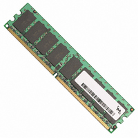
MT9HTF6472AY-40ED4 Micron Technology Inc, MT9HTF6472AY-40ED4 Datasheet - Page 26

MT9HTF6472AY-40ED4
Manufacturer Part Number
MT9HTF6472AY-40ED4
Description
MODULE DDR2 512MB 240-DIMM
Manufacturer
Micron Technology Inc
Specifications of MT9HTF6472AY-40ED4
Memory Type
DDR2 SDRAM
Memory Size
512MB
Speed
400MT/s
Package / Case
240-DIMM
Main Category
DRAM Module
Sub-category
DDR2 SDRAM
Module Type
240RDIMM
Device Core Size
72b
Organization
64Mx72
Total Density
512MByte
Chip Density
512Mb
Access Time (max)
60ps
Maximum Clock Rate
400MHz
Operating Supply Voltage (typ)
1.8V
Operating Current
1.035A
Number Of Elements
9
Operating Supply Voltage (max)
1.9V
Operating Supply Voltage (min)
1.7V
Operating Temp Range
0C to 85C
Operating Temperature Classification
Commercial
Pin Count
240
Mounting
Socket
Lead Free Status / RoHS Status
Lead free / RoHS Compliant
Input Electrical Characteristics and Operating Conditions
Table 10:
Table 11:
I
Table 12:
pdf: 09005aef80e6f860, source: 09005aef80e5b799
HTF9C32_64_128x72AG_2.fm - Rev. C 6/05 EN
Parameter
Parameter
I
Input High (Logic 1) Voltage
Input Low (Logic 0) Voltage
Input High (Logic 1) Voltage
Input Low (Logic 0) Voltage (-40E/-53E)
Input Low (Logic 0) Voltage (-667)
CL (I
t
t
t
t
t
t
t
t
DD
DD
RCD (I
RC (I
RRD (I
CK (I
RAS MIN (I
RAS MAX (I
RP (I
RFC (I
Parameter
DD
DD
DD
DD
Specifications and Conditions
DD
)
DD
DD
)
)
)
)
)
)
DD
DD
Input DC Logic Levels
All voltages referenced to V
Input AC Logic Levels
All voltages referenced to V
General I
)
)
DD
I
V
Input slew rate is specified by AC Parametric Test Conditions. I
fied with ODT disabled. Data bus consists of DQ, DM, DQS, DQS#. I
met with all combinations of EMR bits 10 and 11.
• Definitions for I
• LOW is defined as V
• HIGH is defined as V
• STABLE is defined as inputs stable at a HIGH or LOW level
• FLOATING is defined as inputs at V
• SWITCHING is defined as inputs changing between HIGH and LOW every other clock
• Switching is defined as inputs changing between HIGH and LOW every other data
Parameters
DD
DD
cycle (once per two clocks) for address and control signals
transfer (once per clock) for DQ signals not including masks or strobes
256MB, 512MB, 1GB (x72, SR, ECC) 240-Pin DDR2 SDRAM UDIMM
specifications are tested after the device is properly initialized. 0°C ≤ T
= V
DD
Q = V
SS
SS
Input Electrical Characteristics and Operating Conditions
256MB
512MB
1GB
DD
DD
L = +1.8V ±0.1V; V
Conditions:
IN
IN
≤ V
≥ V
IL
IH
26
(AC) (MAX)
(AC) (MIN)
70,000
127.5
Symbol
-667
Symbol
105
V
V
7.5
V
V
V
15
55
45
15
75
5
3
IH
IL
IH
REF
IL
IL
(
(
(
(
REF
(
DC
DC
AC
AC
AC
Micron Technology, Inc., reserves the right to change products or specifications without notice.
=V
)
)
)
)
)
= V
DD
DD
V
Q/2.
V
REF
REF
Q/2
70,000
MIN
-300
MIN
127.5
-53E
3.75
105
7.5
15
55
45
15
75
+ 125
–
–
+ 250
4
©2003, 2004, 2005 Micron Technology, Inc. All rights reserved.
V
V
V
V
DD
REF
REF
REF
MAX
MAX
70,000
Q + 300
DD
127.5
-40E
105
7.5
-
- 125
15
55
40
15
75
- 250
- 250
3
5
parameters are speci-
DD
values must be
Units
Units
mV
mV
mV
mV
mV
CASE
Units
t
≤ +85°C.
ns
ns
ns
ns
ns
ns
ns
ns
ns
ns
CK
Notes
Notes


