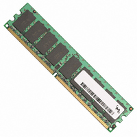
MT9HTF6472AY-40ED4 Micron Technology Inc, MT9HTF6472AY-40ED4 Datasheet - Page 24

MT9HTF6472AY-40ED4
Manufacturer Part Number
MT9HTF6472AY-40ED4
Description
MODULE DDR2 512MB 240-DIMM
Manufacturer
Micron Technology Inc
Specifications of MT9HTF6472AY-40ED4
Memory Type
DDR2 SDRAM
Memory Size
512MB
Speed
400MT/s
Package / Case
240-DIMM
Main Category
DRAM Module
Sub-category
DDR2 SDRAM
Module Type
240RDIMM
Device Core Size
72b
Organization
64Mx72
Total Density
512MByte
Chip Density
512Mb
Access Time (max)
60ps
Maximum Clock Rate
400MHz
Operating Supply Voltage (typ)
1.8V
Operating Current
1.035A
Number Of Elements
9
Operating Supply Voltage (max)
1.9V
Operating Supply Voltage (min)
1.7V
Operating Temp Range
0C to 85C
Operating Temperature Classification
Commercial
Pin Count
240
Mounting
Socket
Lead Free Status / RoHS Status
Lead free / RoHS Compliant
Command Truth Tables
Table 7:
pdf: 09005aef80e6f860, source: 09005aef80e5b799
HTF9C32_64_128x72AG_2.fm - Rev. C 6/05 EN
Function
Mode Register Set
Refresh
Self Refresh Entry
Self Refresh Exit
Single Device Bank
Precharge
ALL Device Banks
Precharge
Device Bank Activate
Write
Write with Auto
Precharge
Read
Read with Auto
Precharge
No Operation
Device Deselect
Power-Down Entry
Power-Down Exit
Notes: 1, 5, 6
Commands Truth Table
Notes: 1. All DDR2 SDRAM device commands are defined by states of S#, RAS#, CAS#, WE#, and CKE
Previous
Cycle
H
H
H
H
H
H
H
H
H
H
H
H
H
Table 7, Commands Truth Table provides a quick reference of DDR2 SDRAM device
available commands. Refer to the 256Mb, 512Mb, or 1Gb DDR2 SDRAM component
data sheet for more Truth Table definitions, including CKE power-down modes and
device bank-to-bank commands.
L
L
2. Device Bank addresses (BA) BA0–BA1/BA2 determine which device bank is to be operated
3. Burst reads or writes at BL = 4 cannot be terminated or interrupted. Refer to the 256Mb,
4. The Power Down Mode does not perform any refresh operations. The duration of power-
5. The state of ODT does not affect the states described in this table. The ODT function is not
6. “X” means “H or L” (but a defined logic level).
7. Self refresh exit is asynchronous.
8. BA2 valid for 1GB only; A13 valid for 512MB and 1GB only.
CKE
256MB, 512MB, 1GB (x72, SR, ECC) 240-Pin DDR2 SDRAM UDIMM
at the rising edge of the clock.
upon. For EMR, BA selects an extended mode register.
512Mb, or 1Gb DDR2 SDRAM discrete data sheet for other restrictions or details.
down is therefore limited by the refresh requirements outlined in the AC parametric sec-
tion.
available during self refresh. Refer to the 256Mb, 512Mb, or 1Gb DDR2 SDRAM discrete
data sheet for other restrictions or details.
Current
Cycle
H
H
H
H
H
H
H
H
H
H
H
X
X
L
L
S#
H
H
H
X
L
L
L
L
L
L
L
L
L
L
L
L
L
L
RAS# CAS#
X
H
H
H
H
H
H
X
X
H
X
H
L
L
L
L
L
L
24
X
H
H
H
H
H
X
X
H
X
H
L
L
L
L
L
L
L
Micron Technology, Inc., reserves the right to change products or specifications without notice.
WE#
H
H
X
H
H
H
H
H
X
X
H
X
H
L
L
L
L
L
BA2
BA1,
BA0
BA
BA
BA
BA
BA
BA
BA
X
X
X
X
X
X
X
X
X
X
X
8
,
Column
Address
Column
Address
Column
Address
Column
Address
A13
A11
©2003, 2004, 2005 Micron Technology, Inc. All rights reserved.
X
X
X
X
X
X
X
X
X
X
X
X
Command Truth Tables
8
–
Row Address
OP Code
A10
X
X
X
X
H
H
H
X
X
X
X
X
X
L
L
L
Address
Address
Address
Address
Column
Column
Column
Column
A9–A0
X
X
X
X
X
X
X
X
X
X
X
X
Notes
2, 3
2, 3
2, 3
2, 3
2
2
2
4
4
7


