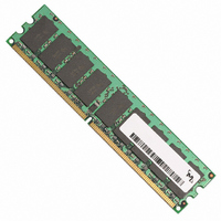
MT9HTF6472AY-40ED4 Micron Technology Inc, MT9HTF6472AY-40ED4 Datasheet - Page 12

MT9HTF6472AY-40ED4
Manufacturer Part Number
MT9HTF6472AY-40ED4
Description
MODULE DDR2 512MB 240-DIMM
Manufacturer
Micron Technology Inc
Specifications of MT9HTF6472AY-40ED4
Memory Type
DDR2 SDRAM
Memory Size
512MB
Speed
400MT/s
Package / Case
240-DIMM
Main Category
DRAM Module
Sub-category
DDR2 SDRAM
Module Type
240RDIMM
Device Core Size
72b
Organization
64Mx72
Total Density
512MByte
Chip Density
512Mb
Access Time (max)
60ps
Maximum Clock Rate
400MHz
Operating Supply Voltage (typ)
1.8V
Operating Current
1.035A
Number Of Elements
9
Operating Supply Voltage (max)
1.9V
Operating Supply Voltage (min)
1.7V
Operating Temp Range
0C to 85C
Operating Temperature Classification
Commercial
Pin Count
240
Mounting
Socket
Lead Free Status / RoHS Status
Lead free / RoHS Compliant
Figure 4:
pdf: 09005aef80e6f860, source: 09005aef80e5b799
HTF9C32_64_128x72AG_2.fm - Rev. C 6/05 EN
COMMAND
ADDRESS
DQS
V
DM
ODT
DQ
V
CK#
CKE
V
V
V
DD
DDL
CK
Rtt
TT
REF
DD
9
Q
7
7
1
7
LOW LEVEL
LVCMOS
DON’T CARE
High-Z
High-Z
High-Z
t
VTD
1
T0
8
LOW LEVEL
t
SSTL_18
CL
Power-up:
V
clock (CK, CK#)
DD
t
DDR2 Power-Up and Initialization
CK
and stable
T = 200µs (min)
Indicates a break in
time scale
t
CL
8
Notes: 1. V
NOP 2
Ta0
T = 400ns (min)
10. A10 should be HIGH at states Tb0 and Tg0 to ensure a PRECHARGE (all banks) command is
11. Bits E7, E8, and E9 must be set to 1 to set OCD default.
12. Bits E7, E8, and E9 must be set to 0 to set OCD exit and all other operating parameters of
2. Apply V
3. Either a NOP or DESELECT command may be applied.
4. 200 cycles of clock (CK, CK#) are required before a READ command can be issued. CKE
5. Two or more REFRESH commands are required.
6. Bits E7, E8, and E9 must all be set to 0 with all other operating parameters of EMRS set as
7. PRE = PRECHARGE command, LM = LOAD MODE command, REF = REFRESH command, ACT
8. DM represents all DM. DQS represents all DQS, DQS#, RDQS,and RDQS# (RDQS/RDQS# only
9. CKE pin uses LVCMOS input levels prior to state T0. After state T0, CKE pin uses SSTL_18
256MB, 512MB, 1GB (x72, SR, ECC) 240-Pin DDR2 SDRAM UDIMM
zero to avoid device latch-up.
The time from when V
to or less than 20ms. One of the following two conditions (a or b) MUST be met:
any V
must be HIGH the entire time.
required.
= ACTIVE command, RA = Row Address, BA = Bank Address.
functional on RDIMMs using x8 components). DQ represents all DQ.
input levels.
issued.
EMRS set as required.
A10 = 1
A.
Tb0
B.
PRE
TT
is not applied directly to the device; however,
t
RPA
DD
V
V
V
Apply V
Apply V
DD
TT
REF
EMR(2)
DD
CODE
supply can not exceed 0.3V.
Tc0
LM
, V
may be 0.95V maximum during power up.
Q before or at the same time as V
tracks V
t MRD
DD
DD
DD
L, and V
EMR(3)
L before or at the same time as V
CODE
Td0
LM
before or at the same time as V
DD
t MRD
Q/2.
DLL Enable
DD
DD
EMR with
CODE
Te0
LM
first starts to power-up to the completion of V
Q are driven from a single power converter output.
t MRD
12
5
DLL Reset
MR with
CODE
Tf0
LM
t MRD
Micron Technology, Inc., reserves the right to change products or specifications without notice.
A10 = 1
Tg0
PRE
t
RPA
TT
200 cycles of CK
and V
Th0
REF
DD
DD
t RFC
t
VTD should be greater than or equal to
L.
Q.
3
REF
See note 4
REF
Ti0
. The voltage difference between
©2003, 2004, 2005 Micron Technology, Inc. All rights reserved.
t RFC
DLL Reset
MR w/o
CODE
Tj0
LM
t MRD
OCD Default 10
EMR with
CODE
Tk0
LM
DD
Initialization
Q must be equal
t MRD
OCD Exit 11
EMR with
CODE
LM
Tl0
t MRD
Operation
Normal
VALID
VALID 3
Tm0
See
note
3


