MT9HTF6472AY-40ED4 Micron Technology Inc, MT9HTF6472AY-40ED4 Datasheet - Page 18
MT9HTF6472AY-40ED4
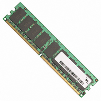
Manufacturer Part Number
MT9HTF6472AY-40ED4
Description
MODULE DDR2 512MB 240-DIMM
Manufacturer
Micron Technology Inc
Specifications of MT9HTF6472AY-40ED4
Memory Type
DDR2 SDRAM
Memory Size
512MB
Speed
400MT/s
Package / Case
240-DIMM
Main Category
DRAM Module
Sub-category
DDR2 SDRAM
Module Type
240RDIMM
Device Core Size
72b
Organization
64Mx72
Total Density
512MByte
Chip Density
512Mb
Access Time (max)
60ps
Maximum Clock Rate
400MHz
Operating Supply Voltage (typ)
1.8V
Operating Current
1.035A
Number Of Elements
9
Operating Supply Voltage (max)
1.9V
Operating Supply Voltage (min)
1.7V
Operating Temp Range
0C to 85C
Operating Temperature Classification
Commercial
Pin Count
240
Mounting
Socket
Lead Free Status / RoHS Status
Lead free / RoHS Compliant


Extended Mode Register (EMR)
DLL Enable/Disable
Output Drive Strength
pdf: 09005aef80e6f860, source: 09005aef80e5b799
HTF9C32_64_128x72AG_2.fm - Rev. C 6/05 EN
The extended mode register controls functions beyond those controlled by the mode
register; these additional functions are DLL enable/disable, output drive strength, ODT
(R
DQS# enable/disable, RDQS/RDQS# enable/disable, and OUTPUT disable/enable.
These functions are controlled via the bits shown in Figure 7, Extended Mode Register
Definition. The extended mode register is programmed via the LOAD MODE (LM) com-
mand and will retain the stored information until it is programmed again or the device
loses power. Reprogramming the extended mode register will not alter the contents of
the memory array, provided it is performed correctly.
The extended mode register must be loaded when all banks are idle and no bursts are in
progress, and the controller must wait the specified time
sequent operation. Violating either of these requirements could result in unspecified
operation.
The DLL may be enabled or disabled by programming bit E0 during the LOAD MODE
command as shown in Figure 7, Extended Mode Register Definition. The DLL must be
enabled for normal operation. DLL enable is required during power-up initialization
and upon returning to normal operation after having disabled the DLL for the purpose
of debugging or evaluation. Enabling the DLL should always be followed by resetting the
DLL using a LOAD MODE command.
The DLL is automatically disabled when entering self refresh operation and is automati-
cally re-enabled and reset upon exit of self refresh operation.
Any time the DLL is enabled (and subsequently reset), 200 clock cycles must occur
before a READ command can be issued to allow time for the internal clock to be syn-
chronized with the external clock. Failing to wait for synchronization to occur may result
in a violation of the
The output drive strength is defined by bit E1 as shown in Figure 7, Extended Mode Reg-
ister Definition. The normal drive strength for all outputs are specified to be SSTL_18.
Programming bit E1 = 0 selects normal (100 percent) drive strength for all outputs.
Selecting a reduced drive strength option (bit E1 = 1) will reduce all outputs to approxi-
mately 60 percent of the SSTL_18 drive strength. This option is intended for the support
of the lighter load and/or point-to-point environments.
TT
256MB, 512MB, 1GB (x72, SR, ECC) 240-Pin DDR2 SDRAM UDIMM
), Posted CAS additive latency (AL), off-chip driver impedance calibration (OCD),
t
AC or
t
DQSCK parameters.
18
Micron Technology, Inc., reserves the right to change products or specifications without notice.
Extended Mode Register (EMR)
©2003, 2004, 2005 Micron Technology, Inc. All rights reserved.
t
MRD before initiating any sub-
Related parts for MT9HTF6472AY-40ED4
Image
Part Number
Description
Manufacturer
Datasheet
Request
R

Part Number:
Description:
IC SDRAM 64MBIT 133MHZ 54TSOP
Manufacturer:
Micron Technology Inc
Datasheet:

Part Number:
Description:
IC SDRAM 64MBIT 5.5NS 86TSOP
Manufacturer:
Micron Technology Inc
Datasheet:
Part Number:
Description:
IC SDRAM 64MBIT 200MHZ 86TSOP
Manufacturer:
Micron Technology Inc
Datasheet:
Part Number:
Description:
IC SDRAM 64MBIT 133MHZ 54TSOP
Manufacturer:
Micron Technology Inc
Datasheet:
Part Number:
Description:
IC SDRAM 128MBIT 133MHZ 54TSOP
Manufacturer:
Micron Technology Inc
Datasheet:

Part Number:
Description:
IC SDRAM 256MBIT 133MHZ 90VFBGA
Manufacturer:
Micron Technology Inc
Datasheet:
Part Number:
Description:
IC SDRAM 128MBIT 133MHZ 54TSOP
Manufacturer:
Micron Technology Inc
Datasheet:
Part Number:
Description:
IC SDRAM 256MBIT 133MHZ 54TSOP
Manufacturer:
Micron Technology Inc
Datasheet:

Part Number:
Description:
IC DDR SDRAM 512MBIT 6NS 66TSOP
Manufacturer:
Micron Technology Inc
Datasheet:
Part Number:
Description:
IC SDRAM 128MBIT 167MHZ 86TSOP
Manufacturer:
Micron Technology Inc
Datasheet:
Part Number:
Description:
IC SDRAM 128MBIT 143MHZ 86TSOP
Manufacturer:
Micron Technology Inc
Datasheet:

Part Number:
Description:
SDRAM 256M-BIT 1.8V 54-PIN VFBGA
Manufacturer:
Micron Technology Inc
Datasheet:
Part Number:
Description:
IC SDRAM 128MBIT 143MHZ 86TSOP
Manufacturer:
Micron Technology Inc
Datasheet:

Part Number:
Description:
IC SDRAM 128MBIT 125MHZ 54VFBGA
Manufacturer:
Micron Technology Inc
Datasheet:
Part Number:
Description:
IC SDRAM 128MBIT 125MHZ 54VFBGA
Manufacturer:
Micron Technology Inc
Datasheet: