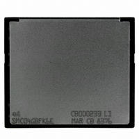
SMC04GBFK6E NUMONYX, SMC04GBFK6E Datasheet - Page 47

SMC04GBFK6E
Manufacturer Part Number
SMC04GBFK6E
Description
MEMORY CARD 4GB COMPACT FLASH
Manufacturer
NUMONYX
Datasheet
1.SMC04GBFK6E.pdf
(90 pages)
Specifications of SMC04GBFK6E
Memory Size
4GB
Memory Type
CompactFLASH
Lead Free Status / RoHS Status
Lead free / RoHS Compliant
SMCxxxBF
9
9.1
Table 41.
1. -REG signal is mode dependent. It must be Low when the card operates in I/O mode and High when it operates in memory
mode.
Error/feature register
Error/feature register
Error/feature register
Word data register
Even data register
Odd data register
Odd data register
Data register
CF-ATA registers
The following section describes the hardware registers used by the host software to issue
commands to the card. These registers are collectively referred to as the ‘task file’.
In accordance with the PCMCIA specification, each register that is located at an odd offset
address can be accessed in the PC card memory or PC card I/O modes. The register can
be addressed in two ways:
In true IDE mode, the size of the transfer is based solely on the register being addressed. All
registers are 8-bit only except for the data register, which is normally 16 bits. However, they
can be configured to be accessed in 8-bit mode for non-DMA operations, by using a Set
Features command (see
Data register
The data register is located at address 1F0h [170h], offset 0h, 8h, and 9h.
The data register is a 16-bit register used to transfer data blocks between the card data
buffer and the host. This register overlaps the error register.
describes the combinations of data register access and explains the overlapped data and
error/feature registers. Because of the overlapped registers, access to the 1F1h, 171h or
offset 1 are not defined for word (–CE2 and –CE1 set to ‘0’) operations, and are treated as
accesses to the word data register. The duplicated registers at offsets 8, 9 and Dh have no
restrictions on the operations that can be performed.
Data register access
Using the normal register address
Using the corresponding even address (normal address -1) when -CE1 is High and -
CE2 Low, unless -IOIS16 is High (not asserted by the card) and an I/O cycle is in
progress. Register data are input or output on data bus lines D15-D8.
(memory and I/O mode)
Section
–CE2
1
1
0
1
0
0
0
10.17).
–CE1
0
0
0
1
0
1
0
A0
X
X
X
X
0
1
1
-REG
-
-
-
-
-
-
-
Table 41
(1)
0h, 8h, 9h
1h, Dh
Offset
0h, 8h
8h, 9h
and
Dh
9h
1h
CF-ATA registers
Table 42
D15 to D0
D15 to D8
D15 to D8
D15 to D8
Data bus
D7 to D0
D7 to D0
D7 to D0
47/90


