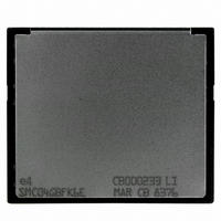
SMC04GBFK6E NUMONYX, SMC04GBFK6E Datasheet - Page 42

SMC04GBFK6E
Manufacturer Part Number
SMC04GBFK6E
Description
MEMORY CARD 4GB COMPACT FLASH
Manufacturer
NUMONYX
Datasheet
1.SMC04GBFK6E.pdf
(90 pages)
Specifications of SMC04GBFK6E
Memory Size
4GB
Memory Type
CompactFLASH
Lead Free Status / RoHS Status
Lead free / RoHS Compliant
Software interface
8
8.1
8.2
42/90
Software interface
CF-ATA drive register set definition and protocol
The CompactFlash memory card can be configured as a high performance I/O device
through:
Communication to or from the card is done using the task file registers which provide all the
necessary registers for control and status information. The PCMCIA interface connects
peripherals to the host using four-register mapping methods.
description of these methods:
Table 36.
Memory mapped addressing
When the card registers are accessed via memory references, the registers appear in the
common memory space window: 0-2 Kbytes as shown in
the data register FIFO. It does not allow random access to the data buffer within the card.
Register 0 is accessed with –CE1 and –CE2 Low, as a word register on the combined odd
and even data bus (D15 to D0). It can also be accessed with –CE1 Low and –CE2 High, by
a pair of byte accesses to offset 0. The address space of this word register overlaps the
address space of the error and feature byte-wide registers at offset 1. When accessed twice
as byte register with –CE1 Low, the first byte is the even byte of the word and the second is
the odd byte. A byte access to address 0 with –CE1 High and –CE2 Low accesses the error
(read) or feature (write) register.
Registers at offset 8, 9 and D are non-overlapping duplicates of the registers at offset 0 and
1. Register 8 is equivalent to register 0, while register 9 accesses the odd byte. Therefore, if
the registers are byte accessed in the order 9 then 8 the data will be transferred odd byte
then even byte. Repeated byte accesses to register 8 or 0 will access consecutive (even
then odd) bytes from the data buffer. Repeated word accesses to register 8, 9 or 0 will
access consecutive words from the data buffer, however repeated byte accesses to register
9 are not supported. Repeated alternating byte accesses to registers 8 then 9 will access
consecutive (even then odd) bytes from the data buffer.
Config index
Standard PC-AT disk I/O address spaces
–
–
Any system decoded 16-byte I/O block using any available IRQ
Memory space.
0
1
2
3
1F0h-1F7h, 3F6h-3F7h (primary);
170h-177h, 376h-377h (secondary) with IRQ 14 (or other available IRQ).
I/O configurations
I/O or memory
Memory
I/O
I/O
I/O
Standards configurations
1F0-1F7h, 3F6h-3F7h
170-177h, 376h-377h
0h-Fh, 400h-7FFh
xx0h-xxFh
Address
I/O mapped 16 continuous registers
Table
Table 36
Secondary I/O mapped
37. This window accesses
Primary I/O mapped
Memory mapped
Description
is a detailed
SMCxxxBF


