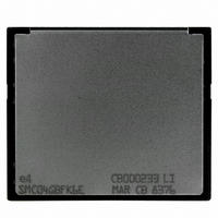
SMC04GBFK6E NUMONYX, SMC04GBFK6E Datasheet - Page 45

SMC04GBFK6E
Manufacturer Part Number
SMC04GBFK6E
Description
MEMORY CARD 4GB COMPACT FLASH
Manufacturer
NUMONYX
Datasheet
1.SMC04GBFK6E.pdf
(90 pages)
Specifications of SMC04GBFK6E
Memory Size
4GB
Memory Type
CompactFLASH
Lead Free Status / RoHS Status
Lead free / RoHS Compliant
- Current page: 45 of 90
- Download datasheet (2Mb)
SMCxxxBF
8.4
I/O primary and secondary address configurations
When the system decodes the primary and secondary address configurations, the registers
are accessed in the block of I/O space as shown in
As for the memory mapped addressing, register 0 is accessed with –CE1 Low and –CE2
Low (and A0 don’t care) as a word register on the combined odd and even data bus (D15 to
D0). This register may also be accessed with –CE1 Low and –CE2 High, by a pair of byte
accesses to offset 0. The address space of this word register overlaps the address space of
the error and feature byte-wide registers at offset 1. When accessed twice as byte register
with –CE1 Low, the first byte is the even byte of the word and the second is the odd byte. A
byte access to register 0 with –CE1 High and –CE2 Low accesses the error (read) or feature
(write) register.
Table 39.
–
REG
0
0
0
0
0
0
0
0
0
0
1F(17)h
1F(17)h
1F(17)h
1F(17)h
1F(17)h
1F(17)h
1F(17)h
1F(17)h
3F(37)h
3F(37)h
A9 to
A4
Primary and secondary I/O decoding
A3
0
0
0
0
0
0
0
0
0
0
A2
0
0
0
0
1
1
1
1
1
1
A1
0
0
1
1
0
0
1
1
1
1
A0
0
1
0
1
0
1
0
1
0
1
Select card/head register
Alternate status register
Sector number register
Drive address register
Cylinder high register
Sector count register
Cylinder low register
Even data register
Status register
Error register
–
IORD=0
Table
39.
Select card/head register
Sector number register
Device control register
Cylinder high register
Sector count register
Cylinder low register
Command register
Even data register
Feature register
Software interface
–
Reserved
IOWR=0
45/90
Related parts for SMC04GBFK6E
Image
Part Number
Description
Manufacturer
Datasheet
Request
R

Part Number:
Description:
Numonyx� Embedded Flash Memory J3 V. D
Manufacturer:
Numonyx
Datasheet:

Part Number:
Description:
Manufacturer:
NUMONYX
Datasheet:

Part Number:
Description:
Manufacturer:
NUMONYX
Datasheet:

Part Number:
Description:
Manufacturer:
NUMONYX
Datasheet:


