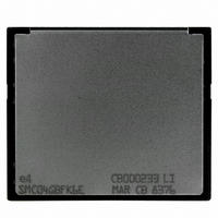
SMC04GBFK6E NUMONYX, SMC04GBFK6E Datasheet - Page 37

SMC04GBFK6E
Manufacturer Part Number
SMC04GBFK6E
Description
MEMORY CARD 4GB COMPACT FLASH
Manufacturer
NUMONYX
Datasheet
1.SMC04GBFK6E.pdf
(90 pages)
Specifications of SMC04GBFK6E
Memory Size
4GB
Memory Type
CompactFLASH
Lead Free Status / RoHS Status
Lead free / RoHS Compliant
- Current page: 37 of 90
- Download datasheet (2Mb)
SMCxxxBF
6.5
Table 32.
1. The
Standby
Read byte access CIS
(8 bits)
Write byte access CIS
(8 bits) invalid
Read byte access
configuration
(8 bits)
Write byte access
configuration
(8 bits)
Read word access CIS
(16 bits)
Write word access CIS
(16 bits) Invalid
Read word access
configuration (16 bits)
Write word access
configuration (16 bits)
Function mode
–
CE signal or both the
Attribute memory function
Attribute memory is a space where identification and configuration information are stored.
Only 8-bit wide accesses at even addresses can be performed in this area. The card
configuration registers are also located in the attribute memory area, at base address 200h.
Attribute memory is not accessible in true IDE mode of operation.
For the attribute memory read function, signals
inactive during the cycle. As in the main memory read functions, the signals
control the even and odd byte address, but only the even byte data is valid during the
attribute memory access. Refer to
Attribute memory function
–REG
–
OE signal and the
X
L
L
L
L
L
L
L
L
–CE2
(1)
H
H
H
H
H
L
L
L
L
–CE1
–
WE signal must be de-asserted between consecutive cycle operations.
(1)
H
L
L
L
L
L
L
L
L
Table 32
A10
X
L
L
L
L
L
L
L
L
A9
for signal states and bus validity.
H
H
H
H
X
L
L
L
L
–
REG and
A0
X
X
X
X
X
L
L
L
L
–OE
(1)
X
H
H
H
H
L
L
L
L
–
OE must be active and
–WE
(1)
H
H
H
H
X
L
L
L
L
High-Z
High-Z
Don’t care Even byte
High-Z
Don’t care Even byte
Not valid
Don’t care Even byte
Not valid
Don’t care Even byte
D15 to D8 D7 to D0
Card configuration
–
CE1 and
High-Z
Even byte
Even byte
Even byte
Even byte
–
WE
–
37/90
CE2
Related parts for SMC04GBFK6E
Image
Part Number
Description
Manufacturer
Datasheet
Request
R

Part Number:
Description:
Numonyx� Embedded Flash Memory J3 V. D
Manufacturer:
Numonyx
Datasheet:

Part Number:
Description:
Manufacturer:
NUMONYX
Datasheet:

Part Number:
Description:
Manufacturer:
NUMONYX
Datasheet:

Part Number:
Description:
Manufacturer:
NUMONYX
Datasheet:


