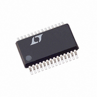
LTC3890EGN-1#TRPBF Linear Technology, LTC3890EGN-1#TRPBF Datasheet - Page 8

LTC3890EGN-1#TRPBF
Manufacturer Part Number
LTC3890EGN-1#TRPBF
Description
IC BUCK SYNC ADJ DUAL 28SSOP
Manufacturer
Linear Technology
Type
Step-Down (Buck)r
Datasheet
1.LTC3890EGN-1TRPBF.pdf
(36 pages)
Specifications of LTC3890EGN-1#TRPBF
Internal Switch(s)
No
Synchronous Rectifier
Yes
Number Of Outputs
2
Voltage - Output
0.8 ~ 24 V
Frequency - Switching
350kHz ~ 535kHz
Voltage - Input
4 ~ 60 V
Operating Temperature
-40°C ~ 125°C
Mounting Type
Surface Mount
Package / Case
28-SSOP
Lead Free Status / RoHS Status
Lead free / RoHS Compliant
Current - Output
-
Power - Output
-
LTC3890-1
PIN FUNCTIONS
ITH1, ITH2 (Pin 1, Pin 13): Error Amplifier Outputs and
Switching Regulator Compensation Points. Each associ-
ated channel’s current comparator trip point increases
with this control voltage.
V
feedback voltage for each controller from an external
resistive divider across the output.
SENSE1
differential current comparators are normally connected
to DCR sensing networks or current sensing resistors.
The ITH pin voltage and controlled offsets between the
SENSE
the current trip threshold.
SENSE1
the Differential Current Comparators. When greater than
INTV
current comparator.
FREQ (Pin 5): The Frequency Control Pin for the Internal
VCO. Connecting the pin to GND forces the VCO to a fixed
low frequency of 350kHz. Connecting the pin to INTV
forces the VCO to a fixed high frequency of 535kHz.
Other frequencies between 50kHz and 900kHz can be
programmed using a resistor between FREQ and GND.
An internal 20μA pull-up current develops the voltage to
be used by the VCO to control the frequency.
PLLIN/MODE (Pin 6): External Synchronization Input to
Phase Detector and Forced Continuous Mode Input. When
an external clock is applied to this pin, the phase-locked
loop will force the rising TG1 signal to be synchronized
with the rising edge of the external clock. When not syn-
chronizing to an external clock, this input, which acts on
8
FB1
, V
CC
–
FB2
– 0.5V, the SENSE
+
–
and SENSE
, SENSE2
, SENSE2
(Pin 2, Pin 12): Receives the remotely sensed
+
–
+
(Pin 3, Pin 11): The (+) input to the
pins in conjunction with R
(Pin 4, Pin 10): The (–) Input to
–
pin supplies current to the
SENSE
set
CC
both controllers, determines how the LTC3890-1 operates
at light loads. Pulling this pin to ground selects Burst Mode
operation. An internal 100k resistor to ground also invokes
Burst Mode Operation when the pin is floated. Tying this
pin to INTV
Tying this pin to a voltage greater than 1.2V and less than
INTV
SGND (Pin 7): Small-signal ground common to both
controllers, must be routed separately from high current
grounds to the common (–) terminals of the C
RUN1, RUN2 (Pin 8, Pin 9): Digital Run Control Inputs
for Each Controller. Forcing RUN1 below 1.16V or RUN2
below 1.20V shuts down that controller. Forcing both of
these pins below 0.7V shuts down the entire LTC3890-1,
reducing quiescent current to approximately 14μA.
INTV
Regulator. The driver and control circuits are powered from
this voltage source. Must be decoupled to power ground
with a minimum of 4.7μF ceramic or other low ESR ca-
pacitor. Do not use the INTV
EXTV
Connected to INTV
bypassing the internal LDO powered from V
EXTV
Applications Information section. Do not float or exceed
14V on this pin.
PGND (Pin 21): Driver Power Ground. Connects to the
sources of bottom (synchronous) N-channel MOSFETs
and the (–) terminal(s) of C
V
be tied between this pin and the signal ground pin.
IN
(Pin 22): Main Supply Pin. A bypass capacitor should
CC
CC
CC
CC
(Pin 19): Output of the Internal Linear Low Dropout
– 1.3V selects pulse-skipping operation.
is higher than 4.7V. See EXTV
(Pin 20): External Power Input to an Internal LDO
CC
forces continuous inductor current operation.
CC
. This LDO supplies INTV
IN
CC
.
pin for any other purpose.
CC
Connection in the
IN
IN
capacitors.
whenever
CC
power,
38901fa


