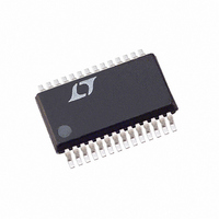
LTC3890EGN-1#TRPBF Linear Technology, LTC3890EGN-1#TRPBF Datasheet - Page 19

LTC3890EGN-1#TRPBF
Manufacturer Part Number
LTC3890EGN-1#TRPBF
Description
IC BUCK SYNC ADJ DUAL 28SSOP
Manufacturer
Linear Technology
Type
Step-Down (Buck)r
Datasheet
1.LTC3890EGN-1TRPBF.pdf
(36 pages)
Specifications of LTC3890EGN-1#TRPBF
Internal Switch(s)
No
Synchronous Rectifier
Yes
Number Of Outputs
2
Voltage - Output
0.8 ~ 24 V
Frequency - Switching
350kHz ~ 535kHz
Voltage - Input
4 ~ 60 V
Operating Temperature
-40°C ~ 125°C
Mounting Type
Surface Mount
Package / Case
28-SSOP
Lead Free Status / RoHS Status
Lead free / RoHS Compliant
Current - Output
-
Power - Output
-
offer much relief. Note that capacitor manufacturers’ ripple
current ratings are often based on only 2000 hours of life.
This makes it advisable to further derate the capacitor, or
to choose a capacitor rated at a higher temperature than
required. Several capacitors may be paralleled to meet
size or height requirements in the design. Due to the high
operating frequency of the LTC3890-1, ceramic capacitors
can also be used for C
if there is any question.
The benefit of the LTC3890-1 2-phase operation can be
calculated by using Equation 1 for the higher power control-
ler and then calculating the loss that would have resulted
if both controller channels switched on at the same time.
The total RMS power lost is lower when both controllers
are operating due to the reduced overlap of current pulses
required through the input capacitor’s ESR. This is why
the input capacitor’s requirement calculated above for the
worst-case controller is adequate for the dual controller
design. Also, the input protection fuse resistance, battery
resistance, and PC board trace resistance losses are also
reduced due to the reduced peak currents in a 2-phase
system. The overall benefit of a multiphase design will
only be fully realized when the source impedance of the
power supply/battery is included in the efficiency testing.
The drains of the top MOSFETs should be placed within
1cm of each other and share a common C
the drains and C
current resonances at V
A small (0.1μF to 1μF) bypass capacitor between the chip
V
also suggested. A 10Ω resistor placed between C
and the V
two channels.
The selection of C
resistance (ESR). Typically, once the ESR requirement
is satisfied, the capacitance is adequate for filtering. The
output ripple (ΔV
where f is the operating frequency, C
capacitance and ΔI
APPLICATIONS INFORMATION
IN
ΔV
pin and ground, placed close to the LTC3890-1, is
OUT
IN
≈ ΔI
pin provides further isolation between the
L
IN
⎛
⎜
⎝
OUT
ESR +
may produce undesirable voltage and
OUT
L
) is approximated by:
is the ripple current in the inductor.
IN
. Always consult the manufacturer
is driven by the effective series
IN
8 • f • C
.
1
OUT
⎞
⎟
⎠
OUT
IN
(s). Separating
is the output
IN
(C1)
The output ripple is highest at maximum input voltage
since ΔI
Setting Output Voltage
The LTC3890-1 output voltages are each set by an exter-
nal feedback resistor divider carefully placed across the
output, as shown in Figure 5. The regulated output voltage
is determined by:
To improve the frequency response, a feedforward ca-
pacitor, C
route the V
inductor or the SW line.
Tracking and Soft-Start (TRACK/SS Pins)
The start-up of each V
the respective TRACK/SS pin. When the voltage on the
TRACK/SS pin is less than the internal 0.8V reference, the
LTC3890-1 regulates the V
the TRACK/SS pin instead of 0.8V. The TRACK/SS pin can
be used to program an external soft-start function or to
allow V
Soft-start is enabled by simply connecting a capacitor
from the TRACK/SS pin to ground, as shown in Figure 6.
An internal 1μA current source charges the capacitor,
providing a linear ramping voltage at the TRACK/SS pin.
The LTC3890-1 will regulate the V
according to the voltage on the TRACK/SS pin, allowing
V
The total soft-start time will be approximately:
OUT
V
t
SS
OUT
to rise smoothly from 0V to its final regulated value.
= C
OUT
L
= 0.8V 1+
FF
increases with input voltage.
SS
, may be used. Great care should be taken to
FB
to track another supply during start-up.
•
line away from noise sources, such as the
Figure 5. Setting Output Voltage
0.8V
1/2 LTC3890-1
1μA
⎛
⎜
⎝
R
R
OUT
B
A
V
FB
⎞
⎟
⎠
FB
is controlled by the voltage on
pin voltage to the voltage on
V
OUT
R
R
38901 F05
B
A
FB
LTC3890-1
pin (and hence V
C
FF
19
38901fa
OUT
)


