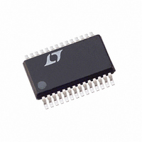
LTC3890EGN-1#TRPBF Linear Technology, LTC3890EGN-1#TRPBF Datasheet - Page 27

LTC3890EGN-1#TRPBF
Manufacturer Part Number
LTC3890EGN-1#TRPBF
Description
IC BUCK SYNC ADJ DUAL 28SSOP
Manufacturer
Linear Technology
Type
Step-Down (Buck)r
Datasheet
1.LTC3890EGN-1TRPBF.pdf
(36 pages)
Specifications of LTC3890EGN-1#TRPBF
Internal Switch(s)
No
Synchronous Rectifier
Yes
Number Of Outputs
2
Voltage - Output
0.8 ~ 24 V
Frequency - Switching
350kHz ~ 535kHz
Voltage - Input
4 ~ 60 V
Operating Temperature
-40°C ~ 125°C
Mounting Type
Surface Mount
Package / Case
28-SSOP
Lead Free Status / RoHS Status
Lead free / RoHS Compliant
Current - Output
-
Power - Output
-
APPLICATIONS INFORMATION
4. Are the SENSE
5. Is the INTV
6. Keep the switching nodes (SW1, SW2), top gate nodes
7. Use a modified star ground technique: a low impedance,
PC Board Layout Debugging
Start with one controller on at a time. It is helpful to use
a DC-50MHz current probe to monitor the current in the
inductor while testing the circuit. Monitor the output switch-
ing node (SW pin) to synchronize the oscilloscope to the
internal oscillator and probe the actual output voltage as
well. Check for proper performance over the operating
voltage and current range expected in the application.
The frequency of operation should be maintained over the
input voltage range down to dropout and until the output
load drops below the low current operation threshold—
typically 25% of the maximum designed current level in
Burst Mode operation.
The duty cycle percentage should be maintained from cycle
to cycle in a well-designed, low noise PCB implementa-
tion. Variation in the duty cycle at a subharmonic rate can
minimum PC trace spacing? The filter capacitor between
SENSE
to the IC. Ensure accurate current sensing with Kelvin
connections at the SENSE resistor.
to the IC, between the INTV
pins? This capacitor carries the MOSFET drivers’ cur-
rent peaks. An additional 1μF ceramic capacitor placed
immediately next to the INTV
improve noise performance substantially.
(TG1, TG2), and boost nodes (BOOST1, BOOST2) away
from sensitive small-signal nodes, especially from
the opposites channel’s voltage and current sensing
feedback pins. All of these nodes have very large and
fast moving signals and therefore should be kept on
the output side of the LTC3890-1 and occupy minimum
PC trace area.
large copper area central grounding point on the same
side of the PC board as the input and output capacitors
with tie-ins for the bottom of the INTV
capacitor, the bottom of the voltage feedback resistive
divider and the SGND pin of the IC.
+
and SENSE
CC
–
decoupling capacitor connected close
and SENSE
–
should be as close as possible
+
CC
leads routed together with
CC
and PGND pins can help
and the power ground
CC
decoupling
suggest noise pickup at the current or voltage sensing
inputs or inadequate loop compensation. Overcompensa-
tion of the loop can be used to tame a poor PC layout if
regulator bandwidth optimization is not required. Only after
each controller is checked for its individual performance
should both controllers be turned on at the same time.
A particularly difficult region of operation is when one
controller channel is nearing its current comparator trip
point when the other channel is turning on its top MOSFET.
This occurs around 50% duty cycle on either channel due
to the phasing of the internal clocks and may cause minor
duty cycle jitter.
Reduce V
the regulator in dropout. Check the operation of the un-
dervoltage lockout circuit by further lowering V
monitoring the outputs to verify operation.
Investigate whether any problems exist only at higher out-
put currents or only at higher input voltages. If problems
coincide with high input voltages and low output currents,
look for capacitive coupling between the BOOST, SW, TG,
and possibly BG connections and the sensitive voltage
and current pins. The capacitor placed across the current
sensing pins needs to be placed immediately adjacent to
the pins of the IC. This capacitor helps to minimize the
effects of differential noise injection due to high frequency
capacitive coupling. If problems are encountered with
high current output loading at lower input voltages, look
for inductive coupling between C
MOSFET components to the sensitive current and voltage
sensing traces. In addition, investigate common ground
path voltage pickup between these components and the
SGND pin of the IC.
An embarrassing problem, which can be missed in an
otherwise properly working switching regulator, results
when the current sensing leads are hooked up backwards.
The output voltage under this improper hookup will still
be maintained but the advantages of current mode control
will not be realized. Compensation of the voltage loop will
be much more sensitive to component selection. This
behavior can be investigated by temporarily shorting out
the current sensing resistor—don’t worry, the regulator
will still maintain control of the output voltage.
IN
from its nominal level to verify operation of
IN
, Schottky and the top
LTC3890-1
IN
27
while
38901fa


