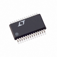
LTC3890EGN-1#TRPBF Linear Technology, LTC3890EGN-1#TRPBF Datasheet - Page 26

LTC3890EGN-1#TRPBF
Manufacturer Part Number
LTC3890EGN-1#TRPBF
Description
IC BUCK SYNC ADJ DUAL 28SSOP
Manufacturer
Linear Technology
Type
Step-Down (Buck)r
Datasheet
1.LTC3890EGN-1TRPBF.pdf
(36 pages)
Specifications of LTC3890EGN-1#TRPBF
Internal Switch(s)
No
Synchronous Rectifier
Yes
Number Of Outputs
2
Voltage - Output
0.8 ~ 24 V
Frequency - Switching
350kHz ~ 535kHz
Voltage - Input
4 ~ 60 V
Operating Temperature
-40°C ~ 125°C
Mounting Type
Surface Mount
Package / Case
28-SSOP
Lead Free Status / RoHS Status
Lead free / RoHS Compliant
Current - Output
-
Power - Output
-
LTC3890-1
A 4.7μH inductor will produce 29% ripple current. The
peak inductor current will be the maximum DC value plus
one half the ripple current, or 5.73A. Increasing the ripple
current will also help ensure that the minimum on-time
of 95ns is not violated. The minimum on-time occurs at
maximum V
The equivalent R
using the minimum value for the maximum current sense
threshold (43mV):
Choosing 1% resistors: R
an output voltage of 3.32V.
The power dissipation on the topside MOSFET can be easily
estimated. Choosing a Fairchild FDS6982S dual MOSFET
results in: R
maximum input voltage with T(estimated) = 50°C:
A short-circuit to ground will result in a folded back cur-
rent of:
with a typical value of R
= 0.125. The resulting power dissipated in the bottom
MOSFET is:
which is less than under full-load conditions.
APPLICATIONS INFORMATION
26
R
P
I
P
t
SC
ON(MIN)
MAIN
SYNC
SENSE
=
0.01Ω
34mV
=
= 3.18A
= 250mW
≤
⎡
⎣ ⎢
(
DS(ON)
3.3V
(
=
IN
22V
0.035Ω
5V – 2.3V
64mV
5.73A
:
V
IN(MAX)
–
SENSE
( )
V
1
5A
2
1
OUT
= 0.035Ω/0.022Ω, C
)
⎛
⎜
⎝
2
)
≈ 0.01Ω
95ns 22V
(
+ 22V
2
resistor value can be calculated by
1.125
( )
⎡ ⎣
+
f
(
4.7μH
DS(ON)
1+ 0.005
2.3V
A
=
(
(
= 25k and R
1
22V 350kHz
)
)
(
2
0.022Ω
and δ = (0.005/°C)(25°C)
⎤
⎦ ⎥
5A
)
(
2
(
3.3V
350kHz
⎞
⎟ = 3.18A
⎠
)
(
(
2.5Ω
50°C – 25°C
MILLER
)
B
)
)
)
= 78.7k yields
= 331mW
(
= 429ns
215pF
= 215pF . At
)
)
⎤ ⎦
•
C
temperature assuming only this channel is on. C
chosen with an ESR of 0.02Ω for low output ripple. The
output ripple in continuous mode will be highest at the
maximum input voltage. The output voltage ripple due to
ESR is approximately:
PC Board Layout Checklist
When laying out the printed circuit board, the following
checklist should be used to ensure proper operation of
the IC. These items are also illustrated graphically in the
layout diagram of Figure 11. Figure 12 illustrates the current
waveforms present in the various branches of the 2-phase
synchronous regulators operating in the continuous mode.
Check the following in your layout:
1. Are the top N-channel MOSFETs MTOP1 and MTOP2
2. Are the signal and power grounds kept separate? The
3. Do the LTC3890-1 V
IN
V
located within 1cm of each other with a common drain
connection at C
decoupling for the two channels as it can cause a large
resonant loop.
combined IC signal ground pin and the ground return
of C
minals. The path formed by the top N-channel MOSFET,
Schottky diode and the C
leads and PC trace lengths. The output capacitor (–)
terminals should be connected as close as possible
to the (–) terminals of the input capacitor by placing
the capacitors next to each other and away from the
Schottky loop described above.
the (+) terminals of C
connected between the (+) terminal of C
ground. The feedback resistor connections should not
be along the high current input feeds from the input
capacitor(s).
is chosen for an RMS current rating of at least 3A at
ORIPPLE
INTVCC
= R
must return to the combined C
ESR
IN
(ΔI
? Do not attempt to split the input
FB
L
OUT
) = 0.02Ω(1.45A) = 29mV
pins’ resistive dividers connect to
? The resistive divider must be
IN
capacitor should have short
OUT
OUT
and signal
(–) ter-
P-P
OUT
38901fa
is


