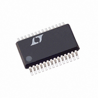
LTC3890EGN-1#TRPBF Linear Technology, LTC3890EGN-1#TRPBF Datasheet - Page 23

LTC3890EGN-1#TRPBF
Manufacturer Part Number
LTC3890EGN-1#TRPBF
Description
IC BUCK SYNC ADJ DUAL 28SSOP
Manufacturer
Linear Technology
Type
Step-Down (Buck)r
Datasheet
1.LTC3890EGN-1TRPBF.pdf
(36 pages)
Specifications of LTC3890EGN-1#TRPBF
Internal Switch(s)
No
Synchronous Rectifier
Yes
Number Of Outputs
2
Voltage - Output
0.8 ~ 24 V
Frequency - Switching
350kHz ~ 535kHz
Voltage - Input
4 ~ 60 V
Operating Temperature
-40°C ~ 125°C
Mounting Type
Surface Mount
Package / Case
28-SSOP
Lead Free Status / RoHS Status
Lead free / RoHS Compliant
Current - Output
-
Power - Output
-
A shorted top MOSFET will result in a high current condition
which will open the system fuse. The switching regulator
will regulate properly with a leaky top MOSFET by altering
the duty cycle to accommodate the leakage.
Phase-Locked Loop and Frequency Synchronization
The LTC3890-1 has an internal phase-locked loop (PLL)
comprised of a phase frequency detector, a lowpass filter,
and a voltage-controlled oscillator (VCO). This allows the
turn-on of the top MOSFET of controller 1 to be locked to
the rising edge of an external clock signal applied to the
PLLIN/MODE pin. The turn-on of controller 2’s top MOSFET
is thus 180 degrees out of phase with the external clock.
The phase detector is an edge sensitive digital type that
provides zero degrees phase shift between the external
and internal oscillators. This type of phase detector does
not exhibit false lock to harmonics of the external clock.
If the external clock frequency is greater than the internal
oscillator’s frequency, f
ously from the phase detector output, pulling up the VCO
input. When the external clock frequency is less than f
current is sunk continuously, pulling down the VCO input.
If the external and internal frequencies are the same but
exhibit a phase difference, the current sources turn on for
an amount of time corresponding to the phase difference.
The voltage at the VCO input is adjusted until the phase
and frequency of the internal and external oscillators are
identical. At the stable operating point, the phase detector
output is high impedance and the internal filter capacitor,
CLP , holds the voltage at the VCO input.
Note that the LTC3890-1 can only be synchronized to an
external clock whose frequency is within range of the
LTC3890-1’s internal VCO, which is nominally 55kHz to
1MHz. This is guaranteed to be between 75kHz and 850kHz.
Typically, the external clock (on the PLLIN/MODE pin) input
high threshold is 1.6V, while the input low threshold is 1.1V.
Rapid phase locking can be achieved by using the FREQ pin
to set a free-running frequency near the desired synchro-
nization frequency. The VCO’s input voltage is prebiased
at a frequency corresponding to the frequency set by the
FREQ pin. Once prebiased, the PLL only needs to adjust
the frequency slightly to achieve phase lock and synchro-
nization. Although it is not required that the free-running
APPLICATIONS INFORMATION
OSC
, then current is sourced continu-
OSC
,
frequency be near external clock frequency, doing so will
prevent the operating frequency from passing through a
large range of frequencies as the PLL locks.
Table 2 summarizes the different states in which the FREQ
pin can be used.
Table 2
Minimum On-Time Considerations
Minimum on-time, t
tion that the LTC3890-1 is capable of turning on the top
MOSFET. It is determined by internal timing delays and the
gate charge required to turn on the top MOSFET. Low duty
cycle applications may approach this minimum on-time
limit and care should be taken to ensure that:
If the duty cycle falls below what can be accommodated
by the minimum on-time, the controller will begin to skip
cycles. The output voltage will continue to be regulated,
but the ripple voltage and current will increase.
Any of the Above
t
ON(MIN)
Figure 10. Relationship Between Oscillator Frequency
and Resistor Value at the FREQ Pin
FREQ PIN
Resistor
INTV
0V
1000
900
800
700
400
300
200
100
600
500
CC
0
<
15
V
V
25
IN
OUT
35 45 55
( )
f
FREQ PIN RESISTOR (kΩ)
ON(MIN)
PLLIN/MODE PIN
External Clock
DC Voltage
DC Voltage
DC Voltage
65 75 85 95 105 115 125
, is the smallest time dura-
LTC3890-1
38901 F10
50kHz to 900kHz
Phase-Locked to
External Clock
FREQUENCY
350kHz
535kHz
23
38901fa


