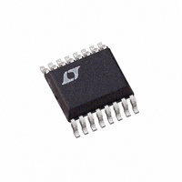
LTC3703EGN Linear Technology, LTC3703EGN Datasheet - Page 7

LTC3703EGN
Manufacturer Part Number
LTC3703EGN
Description
IC BUCK/BOOST SYNC ADJ 5A 16SSOP
Manufacturer
Linear Technology
Type
Step-Down (Buck), Step-Up (Boost)r
Datasheet
1.LTC3703EGNPBF.pdf
(32 pages)
Specifications of LTC3703EGN
Internal Switch(s)
No
Synchronous Rectifier
Yes
Number Of Outputs
1
Voltage - Output
0.8 ~ 93 V
Current - Output
5A
Frequency - Switching
100kHz ~ 600kHz
Voltage - Input
9.3 ~ 100 V
Operating Temperature
-40°C ~ 85°C
Mounting Type
Surface Mount
Package / Case
16-SSOP
Lead Free Status / RoHS Status
Contains lead / RoHS non-compliant
Power - Output
-
Available stocks
Company
Part Number
Manufacturer
Quantity
Price
Company:
Part Number:
LTC3703EGN
Manufacturer:
LINEAR
Quantity:
4
Part Number:
LTC3703EGN
Manufacturer:
LTNEAR
Quantity:
20 000
Company:
Part Number:
LTC3703EGN#PBF
Manufacturer:
LT
Quantity:
3 291
Part Number:
LTC3703EGN#PBF
Manufacturer:
LINEAR/凌特
Quantity:
20 000
Company:
Part Number:
LTC3703EGN#TRPBF
Manufacturer:
LT
Quantity:
3 291
Part Number:
LTC3703EGN#TRPBF
Manufacturer:
LTNEAR
Quantity:
20 000
Company:
Part Number:
LTC3703EGN-5
Manufacturer:
LT
Quantity:
10 000
Part Number:
LTC3703EGN-5
Manufacturer:
LINEAR/凌特
Quantity:
20 000
Company:
Part Number:
LTC3703EGN-5#PBF
Manufacturer:
LT
Quantity:
320
Part Number:
LTC3703EGN-5#PBF
Manufacturer:
LINEAR/凌特
Quantity:
20 000
PIN FUNCTIONS
MODE/SYNC (Pin 1/Pin 6): Pulse-Skip Mode Enable/Sync
Pin. This multifunction pin provides pulse-skip mode
enable/disable control and an external clock input for
synchronization of the internal oscillator. Pulling this pin
below 0.8V or to an external logic-level synchronization
signal disables pulse-skip mode operation and forces
continuous operation. Pulling the pin above 0.8V enables
pulse-skip mode operation. This pin can also be connected
to a feedback resistor divider from a secondary winding
on the inductor to regulate a second output voltage.
f
to this pin sets the free running frequency of the internal
oscillator. See Applications Information section for resistor
value selection details.
COMP (Pin 3/Pin 8): Loop Compensation. This pin is con-
nected directly to the output of the internal error amplifi er.
An RC network is used at the COMP pin to compensate
the feedback loop for optimal transient response.
FB (Pin 4/Pin 9): Feedback Input. Connect FB through a
resistor divider network to V
age. Also connect the loop compensation network from
COMP to FB.
I
the current limit comparator threshold. If the voltage drop
across the bottom MOSFET exceeds the magnitude of the
voltage at I
I
current threshold to be set with a single external resistor
to ground. See the Current Limit Programming section
for more information on choosing R
INV (Pin 6/Pin 11): Top/Bottom Gate Invert. Pulling this pin
above 2V sets the controller to operate in step-up (boost)
mode with the TG output driving the synchronous MOSFET
and the BG output driving the main switch. Below 1V, the
controller will operate in step-down (buck) mode.
RUN/SS (Pin 7/Pin 13): Run/Soft-Start. Pulling RUN/SS
below 0.9V will shut down the LTC3703, turn off both of
the external MOSFET switches and reduce the quiescent
supply current to 50μA. A capacitor from RUN/SS to
ground will control the turn-on time and rate of rise of
the output voltage at power-up. An internal 4μA current
source pull-up at the RUN/SS pin sets the turn-on time
at approximately 750ms/μF .
SET
MAX
MAX
(Pin 2/Pin 7): Frequency Set. A resistor connected
pin has an internal 12μA current source, allowing the
(Pin 5/Pin 10): Current Limit Set. The I
MAX
, the controller goes into current limit. The
(GN16/G28)
OUT
to set the output volt-
IMAX
.
MAX
pin sets
GND (Pin 8/Pin 14): Ground Pin.
BGRTN (Pin 9/Pin 15): Bottom Gate Return. This pin con-
nects to the source of the pull-down MOSFET in the BG driver
and is normally connected to ground. Connecting a negative
supply to this pin allows the synchronous MOSFET’s gate
to be pulled below ground to help prevent false turn-on
during high dV/dt transitions on the SW node. See the
Applications Information section for more details.
BG (Pin 10/Pin 19): Bottom Gate Drive. The BG pin drives
the gate of the bottom N-channel synchronous switch
MOSFET. This pin swings from BGRTN to DRV
DRV
provides power to the BG output driver. This pin should
be connected to a voltage high enough to fully turn on
the external MOSFETs, normally 10V to 15V for standard
threshold MOSFETs. DRV
with a 10μF , low ESR (X5R or better) ceramic capacitor.
V
except the output drivers are powered from this pin. V
should be connected to a low noise power supply voltage
between 9V and 15V and should be bypassed to GND
(Pin 8) with at least a 0.1μF capacitor in close proximity
to the LTC3703.
SW (Pin 13/Pin 26): Switch Node Connection to Inductor
and Bootstrap Capacitor. Voltage swing at this pin is from
a Schottky diode (external) voltage drop below ground
to V
TG (Pin 14/Pin 27): Top Gate Drive. The TG pin drives the
gate of the top N-channel synchronous switch MOSFET.
The TG driver draws power from the BOOST pin and
returns to the SW pin, providing true fl oating drive to the
top MOSFET.
BOOST (Pin 15/Pin 28): Top Gate Driver Supply. The
BOOST pin supplies power to the fl oating TG driver. The
BOOST pin should be bypassed to SW with a low ESR
(X5R or better) 0.1μF ceramic capacitor. An additional fast
recovery Schottky diode from DRV
a complete fl oating charge-pumped supply at BOOST.
V
connected to the high voltage input of the regulator and is
used by the internal feedforward compensation circuitry
to improve line regulation. This is not a supply pin.
CC
IN
IN
(Pin 16/Pin 1): Input Voltage Sense Pin. This pin is
(Pin 12/Pin 21): Main Supply Pin. All internal circuits
CC
.
(Pin 11/Pin 20): Driver Power Supply Pin. DRV
CC
should be bypassed to BGRTN
CC
to BOOST will create
LTC3703
CC
.
3703fb
7
CC
CC


