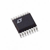
LTC3703EGN Linear Technology, LTC3703EGN Datasheet - Page 17

LTC3703EGN
Manufacturer Part Number
LTC3703EGN
Description
IC BUCK/BOOST SYNC ADJ 5A 16SSOP
Manufacturer
Linear Technology
Type
Step-Down (Buck), Step-Up (Boost)r
Datasheet
1.LTC3703EGNPBF.pdf
(32 pages)
Specifications of LTC3703EGN
Internal Switch(s)
No
Synchronous Rectifier
Yes
Number Of Outputs
1
Voltage - Output
0.8 ~ 93 V
Current - Output
5A
Frequency - Switching
100kHz ~ 600kHz
Voltage - Input
9.3 ~ 100 V
Operating Temperature
-40°C ~ 85°C
Mounting Type
Surface Mount
Package / Case
16-SSOP
Lead Free Status / RoHS Status
Contains lead / RoHS non-compliant
Power - Output
-
Available stocks
Company
Part Number
Manufacturer
Quantity
Price
Company:
Part Number:
LTC3703EGN
Manufacturer:
LINEAR
Quantity:
4
Part Number:
LTC3703EGN
Manufacturer:
LTNEAR
Quantity:
20 000
Company:
Part Number:
LTC3703EGN#PBF
Manufacturer:
LT
Quantity:
3 291
Part Number:
LTC3703EGN#PBF
Manufacturer:
LINEAR/凌特
Quantity:
20 000
Company:
Part Number:
LTC3703EGN#TRPBF
Manufacturer:
LT
Quantity:
3 291
Part Number:
LTC3703EGN#TRPBF
Manufacturer:
LTNEAR
Quantity:
20 000
Company:
Part Number:
LTC3703EGN-5
Manufacturer:
LT
Quantity:
10 000
Part Number:
LTC3703EGN-5
Manufacturer:
LINEAR/凌特
Quantity:
20 000
Company:
Part Number:
LTC3703EGN-5#PBF
Manufacturer:
LT
Quantity:
320
Part Number:
LTC3703EGN-5#PBF
Manufacturer:
LINEAR/凌特
Quantity:
20 000
APPLICATIONS INFORMATION
is above the input supply: V
value of the boost capacitor, C
of the total input capacitance of the topside MOSFET(s).
The reverse breakdown of the external diode, D
greater than V
for the external diode is the reverse recovery and reverse
leakage, either of which may cause excessive reverse cur-
rent to fl ow at full reverse voltage. If the reverse current
times reverse voltage exceeds the maximum allowable
Figure 10c. Secondary Output Loop and V
R1
R2
V
DRV
Figure 10a. V
CC
OPTIONAL V
CONNECTION
10V < V
V
DRV
FCB
GND
CC
CC
LTC3703
+
CC
LTC3703
SEC
BGRTN
1μF
IN(MAX)
< 15V
CC
V
SW
BGRTN
TG
BG
IN
CC
BG1
TG1
SW
V
IN
Generated from 10V < V
. Another important consideration
V
IN
+
V
IN
+
C
BOOST
B
IN
, needs to be 100 times that
L1
C
IN
N
1
= V
12V
T1
IN
12V
CC
OUT
+ V
Connnection
+
< 15V
DRVCC
B
+
+
3703 F10a
, must be
V
10V TO
15V
C
OUT
OUT
3703 F10c
V
1μF
C
V
SEC
OUT
OUT
. The
power dissipation, the diode may be damaged. For best
results, use an ultrafast recovery silicon diode such as
the BAS19.
An internal undervoltage lockout (UVLO) monitors the
voltage on DRV
gate drive voltage. If the DRV
UVLO threshold, the LTC3703 shuts down and the gate
drive outputs remain low.
V
DRV
Figure 10d. Capacitive Charge Pump for V
CC
12V
CC
LTC3703
+
V
DRV
CC
Figure 10b. V
CC
1μF
BGRTN
LTC3703
SW
V
TG
BG
C
IN
IN
CC
BGRTN
+
SW
to ensure that the LTC3703 has suffi cient
V
TG
BG
C
IN
IN
V
IN
+
CC
V
IN
Generated from V
(<40V)
C10
1μF
16V
L1
BAT85
ZHCS400
CC
R17
1M
1%
R17
110k
1%
12V
D2
L1
voltage falls below the
VN2222LL
SW
FB
LT1613
0.22μF
10μH
GND
OUT
LTC3703
L2
CC
SHDN
< 10V
+
(V
V
IN
IN
BAT85
+
BAT85
C
3703 F10d
V
< 40V)
OUT
OUT
17
3703 F10b
C
V
<10V
OUT
OUT
3703fb
C9
4.7μF
6.3V


