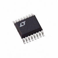
LTC3703EGN Linear Technology, LTC3703EGN Datasheet - Page 20

LTC3703EGN
Manufacturer Part Number
LTC3703EGN
Description
IC BUCK/BOOST SYNC ADJ 5A 16SSOP
Manufacturer
Linear Technology
Type
Step-Down (Buck), Step-Up (Boost)r
Datasheet
1.LTC3703EGNPBF.pdf
(32 pages)
Specifications of LTC3703EGN
Internal Switch(s)
No
Synchronous Rectifier
Yes
Number Of Outputs
1
Voltage - Output
0.8 ~ 93 V
Current - Output
5A
Frequency - Switching
100kHz ~ 600kHz
Voltage - Input
9.3 ~ 100 V
Operating Temperature
-40°C ~ 85°C
Mounting Type
Surface Mount
Package / Case
16-SSOP
Lead Free Status / RoHS Status
Contains lead / RoHS non-compliant
Power - Output
-
Available stocks
Company
Part Number
Manufacturer
Quantity
Price
Company:
Part Number:
LTC3703EGN
Manufacturer:
LINEAR
Quantity:
4
Part Number:
LTC3703EGN
Manufacturer:
LTNEAR
Quantity:
20 000
Company:
Part Number:
LTC3703EGN#PBF
Manufacturer:
LT
Quantity:
3 291
Part Number:
LTC3703EGN#PBF
Manufacturer:
LINEAR/凌特
Quantity:
20 000
Company:
Part Number:
LTC3703EGN#TRPBF
Manufacturer:
LT
Quantity:
3 291
Part Number:
LTC3703EGN#TRPBF
Manufacturer:
LTNEAR
Quantity:
20 000
Company:
Part Number:
LTC3703EGN-5
Manufacturer:
LT
Quantity:
10 000
Part Number:
LTC3703EGN-5
Manufacturer:
LINEAR/凌特
Quantity:
20 000
Company:
Part Number:
LTC3703EGN-5#PBF
Manufacturer:
LT
Quantity:
320
Part Number:
LTC3703EGN-5#PBF
Manufacturer:
LINEAR/凌特
Quantity:
20 000
APPLICATIONS INFORMATION
LTC3703
Feedback Component Selection
Selecting the R and C values for a typical Type 2 or
Type 3 loop is a nontrivial task. The applications shown
in this data sheet show typical values, optimized for the
power components shown. They should give acceptable
performance with similar power components, but can be
way off if even one major power component is changed
signifi cantly. Applications that require optimized transient
response will require recalculation of the compensation
values specifi cally for the circuit in question. The underly-
ing mathematics are complex, but the component values
can be calculated in a straightforward manner if we know
the gain and phase of the modulator at the crossover
frequency.
Modulator gain and phase can be measured directly from a
breadboard or can be simulated if the appropriate parasitic
values are known. Measurement will give more accurate
results, but simulation can often get close enough to give
a working system. To measure the modulator gain and
phase directly, wire up a breadboard with an LTC3703
and the actual MOSFETs, inductor and input and output
capacitors that the fi nal design will use. This breadboard
should use appropriate construction techniques for high
speed analog circuitry: bypass capacitors located close
to the LTC3703, no long wires connecting components,
appropriately sized ground returns, etc. Wire the feedback
amplifi er as a simple Type 1 loop, with a 10k resistor from
V
to FB. Choose the bias resistor, R
desired output voltage. Disconnect R
connect it to a signal generator or to the source output
of a network analyzer to inject a test signal into the loop.
Measure the gain and phase from the COMP pin to the
output node at the positive terminal of the output capacitor.
Make sure the analyzer’s input is AC coupled so that the DC
voltages present at both the COMP and V
corrupt the measurements or damage the analyzer.
If breadboard measurement is not practical, a SPICE
simulation can be used to generate approximate gain/phase
curves. Plug the expected capacitor, inductor and MOSFET
20
OUT
to FB and a 0.1μF feedback capacitor from COMP
B
, as required to set the
B
from ground and
OUT
nodes don’t
values into the following SPICE deck and generate an AC
plot of V(V
degrees. Refer to your SPICE manual for details of how
to generate this plot.
*3703 modulator gain/phase
*2003 Linear Technology
*this fi le written to run with PSpice 8.0
*may require modifi cations for other
SPICE simulators
*MOSFETs
rfet mod sw 0.02
*inductor
lext sw out1 10u
rl out1 out 0.015
*output cap
cout out out2 540u
resr out2 0 0.01
*3703 internals
emod mod 0 value
vstim comp 0 0 ac 1
.ac dec 100 1k 1meg
.probe
.end
With the gain/phase plot in hand, a loop crossover fre-
quency can be chosen. Usually the curves look something
like Figure 11. Choose the crossover frequency in the ris-
ing or fl at parts of the phase curve, beyond the external
LC poles. Frequencies between 10kHz and 50kHz usually
work well. Note the gain (GAIN, in dB) and phase (PHASE,
in degrees) at this point. The desired feedback amplifi er
gain will be –GAIN to make the loop gain at 0dB at this
frequency. Now calculate the needed phase boost, assum-
ing 60° as a target phase margin:
If the required BOOST is less than 60°, a Type 2 loop can
be used successfully, saving two external components.
BOOST values greater than 60° usually require Type 3
loops for satisfactory performance.
BOOST = –(PHASE + 30°)
OUT
)/V(COMP) in dB and phase of V
= {57*v(comp)}
;MOSFET rdson
;inductor value
;inductor series R
;capacitor value
;capacitor ESR
;3703multiplier
;ac stimulus
OUT
3703fb
in


