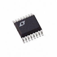
LTC3703EGN Linear Technology, LTC3703EGN Datasheet - Page 23

LTC3703EGN
Manufacturer Part Number
LTC3703EGN
Description
IC BUCK/BOOST SYNC ADJ 5A 16SSOP
Manufacturer
Linear Technology
Type
Step-Down (Buck), Step-Up (Boost)r
Datasheet
1.LTC3703EGNPBF.pdf
(32 pages)
Specifications of LTC3703EGN
Internal Switch(s)
No
Synchronous Rectifier
Yes
Number Of Outputs
1
Voltage - Output
0.8 ~ 93 V
Current - Output
5A
Frequency - Switching
100kHz ~ 600kHz
Voltage - Input
9.3 ~ 100 V
Operating Temperature
-40°C ~ 85°C
Mounting Type
Surface Mount
Package / Case
16-SSOP
Lead Free Status / RoHS Status
Contains lead / RoHS non-compliant
Power - Output
-
Available stocks
Company
Part Number
Manufacturer
Quantity
Price
Company:
Part Number:
LTC3703EGN
Manufacturer:
LINEAR
Quantity:
4
Part Number:
LTC3703EGN
Manufacturer:
LTNEAR
Quantity:
20 000
Company:
Part Number:
LTC3703EGN#PBF
Manufacturer:
LT
Quantity:
3 291
Part Number:
LTC3703EGN#PBF
Manufacturer:
LINEAR/凌特
Quantity:
20 000
Company:
Part Number:
LTC3703EGN#TRPBF
Manufacturer:
LT
Quantity:
3 291
Part Number:
LTC3703EGN#TRPBF
Manufacturer:
LTNEAR
Quantity:
20 000
Company:
Part Number:
LTC3703EGN-5
Manufacturer:
LT
Quantity:
10 000
Part Number:
LTC3703EGN-5
Manufacturer:
LINEAR/凌特
Quantity:
20 000
Company:
Part Number:
LTC3703EGN-5#PBF
Manufacturer:
LT
Quantity:
320
Part Number:
LTC3703EGN-5#PBF
Manufacturer:
LINEAR/凌特
Quantity:
20 000
APPLICATIONS INFORMATION
cycle (minimum V
limit does not kick in at loads < I
Once V
Note that in a boost mode architecture, it is only possible
to provide protection for “soft” shorts where V
For hard shorts, the inductor current is limited only by the
input supply capability. Refer to Current Limit Program-
ming for buck mode for further considerations for current
limit programming.
Boost Converter: Feedback Loop/Compensation
Compensating a voltage mode boost converter is unfor-
tunately more diffi cult than for a buck converter. This is
due to an additional right-half plane (RHP) zero that is
present in the boost converter but not in a buck. The ad-
ditional phase lag resulting from the RHP zero is diffi cult
if not impossible to compensate even with a Type 3 loop,
so the best approach is usually to roll off the loop gain at
a lower frequency than what could be achievable in buck
converter.
A typical gain/phase plot of a voltage mode boost converter
is shown in Figure 16. The modulator gain and phase can
be measured as described for a buck converter or can be
estimated as follows:
Since signifi cant phase shift begins at frequencies above
the dominant LC pole, choose a crossover frequency no
greater than about half this pole frequency. The gain of
the compensation network should equal –GAIN at this
frequency so that the overall loop gain is 0dB here. The
R
GAIN (COMP-to-V
Dominant Pole: f
V
IMAX
PROG
PROG
= V
=
=
⎛
⎜
⎝
1
I
is determined, R
PROG
O MAX
–
V
(
IN MIN
D
V
OUT
MAX
(
/12μA
IN
)
P
) in order to ensure that the current
) )
OUT
R
=
⎞
⎟
⎠
DS ON
I
O MAX
V
V
(
(
DC gain) = 20Log(V
OUT
IN
)
(
IMAX
)
•
1 δ
•
2π
+
R
O(MAX)
DS ON
is chosen as follows:
)
1
LC
(
:
)
(
1 δ
+
OUT
)
OUT
2
/V
> V
IN
)
IN
.
compensation component to achieve this, using a Type 1
amplifi er (see Figure 12), is:
Run/Soft-Start Function
The RUN/SS pin is a multipurpose pin that provide a soft-
start function and a means to shut down the LTC3703.
Soft-start reduces the input supply’s surge current by
gradually increasing the duty cycle and can also be used
for power supply sequencing.
Pulling RUN/SS below 0.9V puts the LTC3703 into a low
quiescent current shutdown (I
driven directly from logic as shown in Figure 17. Releasing
the RUN/SS pin allows an internal 4μA current source to
G = 10
C1 = 1/(2π • f • G • R1)
RUN/SS
2V/DIV
5V/DIV
2A/DIV
GAIN
(dB)
V
A
OUT
Figure 16. Transfer Function of Boost Modulator
V
0
I
L
–GAIN/20
V
I
C
LOAD
IN
SS
Figure 17. LTC3703 Start-Up Operation
= 50V
= 0.01μF
GAIN
PHASE
= 2A
–12dB/OCT
2ms/DIV
Q
≅ 50μA). This pin can be
LTC3703
3703 F17
3703 F16
0
–90
–180
PHASE
(DEG)
23
3703fb


