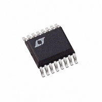
LTC3703EGN Linear Technology, LTC3703EGN Datasheet - Page 19

LTC3703EGN
Manufacturer Part Number
LTC3703EGN
Description
IC BUCK/BOOST SYNC ADJ 5A 16SSOP
Manufacturer
Linear Technology
Type
Step-Down (Buck), Step-Up (Boost)r
Datasheet
1.LTC3703EGNPBF.pdf
(32 pages)
Specifications of LTC3703EGN
Internal Switch(s)
No
Synchronous Rectifier
Yes
Number Of Outputs
1
Voltage - Output
0.8 ~ 93 V
Current - Output
5A
Frequency - Switching
100kHz ~ 600kHz
Voltage - Input
9.3 ~ 100 V
Operating Temperature
-40°C ~ 85°C
Mounting Type
Surface Mount
Package / Case
16-SSOP
Lead Free Status / RoHS Status
Contains lead / RoHS non-compliant
Power - Output
-
Available stocks
Company
Part Number
Manufacturer
Quantity
Price
Company:
Part Number:
LTC3703EGN
Manufacturer:
LINEAR
Quantity:
4
Part Number:
LTC3703EGN
Manufacturer:
LTNEAR
Quantity:
20 000
Company:
Part Number:
LTC3703EGN#PBF
Manufacturer:
LT
Quantity:
3 291
Part Number:
LTC3703EGN#PBF
Manufacturer:
LINEAR/凌特
Quantity:
20 000
Company:
Part Number:
LTC3703EGN#TRPBF
Manufacturer:
LT
Quantity:
3 291
Part Number:
LTC3703EGN#TRPBF
Manufacturer:
LTNEAR
Quantity:
20 000
Company:
Part Number:
LTC3703EGN-5
Manufacturer:
LT
Quantity:
10 000
Part Number:
LTC3703EGN-5
Manufacturer:
LINEAR/凌特
Quantity:
20 000
Company:
Part Number:
LTC3703EGN-5#PBF
Manufacturer:
LT
Quantity:
320
Part Number:
LTC3703EGN-5#PBF
Manufacturer:
LINEAR/凌特
Quantity:
20 000
APPLICATIONS INFORMATION
will approach its ESR and the rolloff due to the capaci-
tor will stop, leaving 6dB/octave and 90° of phase shift
(Figure 11).
So far, the AC response of the loop is pretty well out of the
user’s control. The modulator is a fundamental piece of the
LTC3703 design and the external L and C are usually chosen
based on the regulation and load current requirements
without considering the AC loop response. The feedback
amplifi er, on the other hand, gives us a handle with which
to adjust the AC response. The goal is to have 180° phase
shift at DC (so the loop regulates) and something less than
360° phase shift at the point that the loop gain falls to 0dB.
The simplest strategy is to set up the feedback amplifi er
as an inverting integrator, with the 0dB frequency lower
than the LC pole (Figure 12). This “Type 1” confi guration
is stable but transient response is less than exceptional
if the LC pole is at a low frequency.
Figure 13 shows an improved “Type 2” circuit that uses
an additional pole-zero pair to temporarily remove 90°
of phase shift. This allows the loop to remain stable with
90° more phase shift in the LC section, provided the loop
reaches 0dB gain near the center of the phase “bump.”
IN
R1
R
V
B
REF
FB
Figure 12. Type 1 Schematic and Transfer Function
Figure 11. Transfer Function of Buck Modulator
–
+
C1
A
V
0
PHASE
GAIN
OUT
0
–12dB/OCT
PHASE
GAIN
–6dB/OCT
–6dB/OCT
3703 F11
FREQ
–90
–180
–270
–360
FREQ
–90
–180
–270
–360
3703 F12
Type 2 loops work well in systems where the ESR zero
in the LC roll-off happens close to the LC pole, limiting
the total phase shift due to the LC. The additional phase
compensation in the feedback amplifi er allows the 0dB
point to be at or above the LC pole frequency, improving
loop bandwidth substantially over a simple Type 1 loop.
It has limited ability to compensate for LC combinations
where low capacitor ESR keeps the phase shift near 180°
for an extended frequency range. LTC3703 circuits using
conventional switching grade electrolytic output capaci-
tors can often get acceptable phase margin with Type 2
compensation.
“Type 3” loops (Figure 14) use two poles and two zeros to
obtain a 180° phase boost in the middle of the frequency
band. A properly designed Type 3 circuit can maintain
acceptable loop stability even when low output capacitor
ESR causes the LC section to approach 180° phase shift
well above the initial LC roll-off. As with a Type 2 circuit,
the loop should cross through 0dB in the middle of the
phase bump to maximize phase margin. Many LTC3703
circuits using low ESR tantalum or OS-CON output capaci-
tors need Type 3 compensation to obtain acceptable phase
margin with a high bandwidth feedback loop.
IN
IN
R1
R
B
R1
R
V
B
REF
FB
R3
V
Figure 13. Type 2 Schematic and Transfer Function
Figure 14. Type 3 Schematic and Transfer Function
REF
FB
C3
–
+
R2
–
+
R2
C2
C2
C1
C1
OUT
OUT
0
0
PHASE
GAIN
GAIN
–6dB/OCT
–6dB/OCT
+6dB/OCT
LTC3703
PHASE
–6dB/OCT
–6dB/OCT
19
3703 F13
FREQ
–90
–180
–270
–360
3703fb
3703 F14
FREQ
–90
–180
–270
–360


