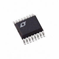
LTC3703EGN Linear Technology, LTC3703EGN Datasheet - Page 27

LTC3703EGN
Manufacturer Part Number
LTC3703EGN
Description
IC BUCK/BOOST SYNC ADJ 5A 16SSOP
Manufacturer
Linear Technology
Type
Step-Down (Buck), Step-Up (Boost)r
Datasheet
1.LTC3703EGNPBF.pdf
(32 pages)
Specifications of LTC3703EGN
Internal Switch(s)
No
Synchronous Rectifier
Yes
Number Of Outputs
1
Voltage - Output
0.8 ~ 93 V
Current - Output
5A
Frequency - Switching
100kHz ~ 600kHz
Voltage - Input
9.3 ~ 100 V
Operating Temperature
-40°C ~ 85°C
Mounting Type
Surface Mount
Package / Case
16-SSOP
Lead Free Status / RoHS Status
Contains lead / RoHS non-compliant
Power - Output
-
Available stocks
Company
Part Number
Manufacturer
Quantity
Price
Company:
Part Number:
LTC3703EGN
Manufacturer:
LINEAR
Quantity:
4
Part Number:
LTC3703EGN
Manufacturer:
LTNEAR
Quantity:
20 000
Company:
Part Number:
LTC3703EGN#PBF
Manufacturer:
LT
Quantity:
3 291
Part Number:
LTC3703EGN#PBF
Manufacturer:
LINEAR/凌特
Quantity:
20 000
Company:
Part Number:
LTC3703EGN#TRPBF
Manufacturer:
LT
Quantity:
3 291
Part Number:
LTC3703EGN#TRPBF
Manufacturer:
LTNEAR
Quantity:
20 000
Company:
Part Number:
LTC3703EGN-5
Manufacturer:
LT
Quantity:
10 000
Part Number:
LTC3703EGN-5
Manufacturer:
LINEAR/凌特
Quantity:
20 000
Company:
Part Number:
LTC3703EGN-5#PBF
Manufacturer:
LT
Quantity:
320
Part Number:
LTC3703EGN-5#PBF
Manufacturer:
LINEAR/凌特
Quantity:
20 000
APPLICATIONS INFORMATION
With most output capacitors, several devices paralleled
to get the ESR down will have so much capacitance that
this drop term is negligible. Ceramic capacitors are an
exception; a small ceramic capacitor can have suitably low
ESR with relatively small values of capacitance, making
this second drop term more signifi cant.
Optimizing Loop Compensation
Loop compensation has a fundamental impact on transient
recovery time, the time it takes the LTC3703 to recover
after the output voltage has dropped due to a load step.
Optimizing loop compensation entails maintaining the high-
est possible loop bandwidth while ensuring loop stability.
The feedback component selection section describes in
detail the techniques used to design an optimized Type 3
feedback loop, appropriate for most LTC3703 systems.
Measurement Techniques
Measuring transient response presents a challenge in
two respects: obtaining an accurate measurement and
generating a suitable transient to test the circuit. Output
measurements should be taken with a scope probe directly
across the output capacitor. Proper high frequency probing
techniques should be used. In particular, don’t use the 6"
ground lead that comes with the probe! Use an adapter that
fi ts on the tip of the probe and has a short ground clip to
ensure that inductance in the ground path doesn’t cause
a bigger spike than the transient signal being measured.
Conveniently, the typical probe tip ground clip is spaced
just right to span the leads of a typical output capacitor.
Now that we know how to measure the signal, we need to
have something to measure. The ideal situation is to use
the actual load for the test and switch it on and off while
watching the output. If this isn’t convenient, a current
step generator is needed. This generator needs to be able
to turn on and off in nanoseconds to simulate a typical
switching logic load, so stray inductance and long clip
leads between the LTC3703 and the transient generator
must be minimized.
Figure 19 shows an example of a simple transient gen-
erator. Be sure to use a noninductive resistor as the load
element—many power resistors use an inductive spiral
pattern and are not suitable for use here. A simple solu-
tion is to take ten 1/4W fi lm resistors and wire them in
parallel to get the desired value. This gives a noninductive
resistive load which can dissipate 2.5W continuously or
50W if pulsed with a 5% duty cycle, enough for most
LTC3703 circuits. Solder the MOSFET and the resistor(s)
as close to the output of the LTC3703 circuit as possible
and set up the signal generator to pulse at a 100Hz rate
with a 5% duty cycle. This pulses the LTC3703 with 500μs
transients10ms apart, adequate for viewing the entire
transient recovery time for both positive and negative
transitions while keeping the load resistor cool.
Design Example
As a design example, take a supply with the following
specifi cations: V
12V ±5%, I
R
Next, choose the inductor value for about 40% ripple
current at maximum V
With 10μH inductor, ripple current will vary from 3.2A to
4A (32% to 40%) over the input supply range.
Next, verify that the minimum on-time is not violated. The
minimum on-time occurs at maximum V
which is above the LTC3703’s 200ns minimum on-time.
SET
R
L
t
ON MIN
SET
=
to give the 250kHz operating frequency:
(
(
250
= 7100/(250 – 25) = 31.6k
)
kHz
OUT(MAX)
=
Figure 19. Transient Load Generator
DUTY CYCLE
LOCATE CLOSE TO THE OUTPUT
V
GENERATOR
12
100Hz, 5%
0V TO 10V
IN MIN
)( . )(
LTC3703
PULSE
V
IN
(
0 4 10
V
OUT
= 36V to 72V (48V nominal), V
)
= 10A, f = 250kHz. First, calculate
( )
IN
f
:
A
=
)
50Ω
72 250
⎛
⎝ ⎜
1
(
–
12
12
72
R
IRFZ44 OR
EQUIVALENT
LOAD
kHz
V
⎞
⎠ ⎟
OUT
=
)
10
3703 F19
LTC3703
=
IN
μH
667
:
ns
27
OUT
3703fb
=


