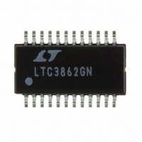
LTC3862IGN#PBF Linear Technology, LTC3862IGN#PBF Datasheet - Page 35

LTC3862IGN#PBF
Manufacturer Part Number
LTC3862IGN#PBF
Description
IC CTRLR DC/DC STPUP 24SSOP
Manufacturer
Linear Technology
Type
Step-Up (Boost)r
Datasheet
1.LTC3862EGNPBF.pdf
(40 pages)
Specifications of LTC3862IGN#PBF
Internal Switch(s)
No
Synchronous Rectifier
No
Number Of Outputs
1
Voltage - Output
1.22 ~ 200 V
Current - Output
50mA
Frequency - Switching
300kHz
Voltage - Input
4 ~ 36 V
Operating Temperature
-40°C ~ 125°C
Mounting Type
Surface Mount
Package / Case
24-SSOP
Primary Input Voltage
36V
No. Of Outputs
1
Output Current
50mA
No. Of Pins
24
Operating Temperature Range
-40°C To +125°C
Msl
MSL 1 - Unlimited
Supply Voltage Range
4V To 36V
Rohs Compliant
Yes
Lead Free Status / RoHS Status
Lead free / RoHS Compliant
Power - Output
-
10. The output resistor divider should be located as
11. Since the inductor acts like a current source in a
12. The SENSE
13. If an external RC fi lter is used between the sense
APPLICATIONS INFORMATION
close as possible to the IC, with the bottom resistor
connected between FB and SGND. The PCB trace
connecting the top resistor to the upper terminal of
the output capacitor should avoid any high frequency
switching nodes.
peak current mode control topology, its placement
on the board is less critical than the high di/dt com-
ponents.
parallel to one another with minimum spacing in be-
tween all the way to the sense resistor. These traces
should avoid any high frequency switching nodes in
the layout. These PCB traces should also be Kelvin-
connected to the interior of the sense resistor pads,
in order to avoid sensing errors due to parasitic PCB
resistance IR drops.
resistor and the SENSE
components should be placed as close as possible to
the SENSE
the SENSE
point where the current sense resistor is grounded.
–
+
+
line is connected to the ground only at the
and SENSE
and SENSE
+
–
–
and SENSE
PCB traces should be routed
pins of the IC. Ensure that
–
pins, these fi lter
14. Keep the MOSFET drain nodes (SW1, SW2) away
15. Check the stress on the power MOSFETs by indepen-
16. When synchronizing the LTC3862 to an external clock,
from sensitive small-signal nodes, especially from
the opposite channel’s current-sensing signals. The
SW nodes can have slew rates in excess of 1V/ns
relative to ground and should therefore be kept on
the “output side” of the LTC3862.
dently measuring the drain-to-source voltages directly
across the devices terminals. Beware of inductive
ringing that could exceed the maximum voltage rating
of the MOSFET. If this ringing cannot be avoided and
exceeds the maximum rating of the device, choose
a higher voltage rated MOSFET or consider using a
snubber.
use a low impedance source such as a logic gate to
drive the SYNC pin and keep the lead as short as
possible.
LTC3862
35
3862fb


