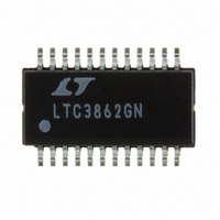
LTC3862IGN#PBF Linear Technology, LTC3862IGN#PBF Datasheet - Page 25

LTC3862IGN#PBF
Manufacturer Part Number
LTC3862IGN#PBF
Description
IC CTRLR DC/DC STPUP 24SSOP
Manufacturer
Linear Technology
Type
Step-Up (Boost)r
Datasheet
1.LTC3862EGNPBF.pdf
(40 pages)
Specifications of LTC3862IGN#PBF
Internal Switch(s)
No
Synchronous Rectifier
No
Number Of Outputs
1
Voltage - Output
1.22 ~ 200 V
Current - Output
50mA
Frequency - Switching
300kHz
Voltage - Input
4 ~ 36 V
Operating Temperature
-40°C ~ 125°C
Mounting Type
Surface Mount
Package / Case
24-SSOP
Primary Input Voltage
36V
No. Of Outputs
1
Output Current
50mA
No. Of Pins
24
Operating Temperature Range
-40°C To +125°C
Msl
MSL 1 - Unlimited
Supply Voltage Range
4V To 36V
Rohs Compliant
Yes
Lead Free Status / RoHS Status
Lead free / RoHS Compliant
Power - Output
-
APPLICATIONS INFORMATION
Maximum Duty Cycle Limitations
Another operating extreme occurs at high duty cycle,
when the input voltage is low and the output voltage is
high. In this case:
A single-ended boost converter needs a minimum off-time
every cycle in order to allow energy transfer from the input
inductor to the output capacitor. This minimum off-time
translates to a maximum duty cycle for the converter. The
equation above can be rearranged to obtain the maximum
output voltage for a given minimum input or maximum
duty cycle.
The equation for D
guideline for determining the maximum duty cycle of
the application circuit. However, losses in the inductor,
input and output capacitors, the power MOSFETs, the
sense resistors and the controller (gate drive losses) all
contribute to an increasing of the duty cycle. The effect
of these losses will be to decrease the maximum output
voltage for a given minimum input voltage.
After the initial calculations have been completed for an
application circuit, it is important to build a prototype of
the circuit and measure it over the entire input voltage
range, from light load to full load, and over temperature,
in order to verify proper operation of the circuit.
Peak and Average Input Currents
The control circuit in the LTC3862 measures the input
current (by means of resistors in the sources of the power
MOSFETs), so the output current needs to be refl ected back
to the input in order to dimension the power MOSFETs
D
V
MAX
O MAX
(
=
)
⎛
⎜
⎝
=
V
1
O
–
+
V
D
V
V
IN
MAX
O
MAX
F
–
+
V
V
–
above can be used as an initial
IN MIN
F
V
(
F
)
⎞
⎟
⎠
properly. Based on the fact that, ideally, the output power
is equal to the input power, the maximum average input
current is:
The peak current in each inductor is:
where n represents the number of phases and χ represents
the percentage peak-to-peak ripple current in the inductor.
For example, if the design goal is to have 30% ripple cur-
rent in the inductor, then χ = 0.30, and the peak current
is 15% greater than the average.
Inductor Selection
Given an input voltage range, operating frequency and
ripple current, the inductor value can be determined using
the following equation:
where:
Choosing a larger value of ΔI
value inductor but results in higher output voltage ripple,
greater core losses, and higher ripple current ratings for
the input and output capacitors. A reasonable starting point
is 30% ripple current in the inductor (χ = 0.3), or:
I
I
L
ΔI
ΔI
IN MAX
IN PK
=
(
(
L
L
V
=
=
Δ
)
IN MIN
χ
0 3
=
I
n
)
(
L
n
.
=
•
n
1
•
1
1
f
•
•
I
I
)
O MAX
O MAX
–
–
⎛
⎝ ⎜
1
•
(
I
(
D
O MAX
1
–
D
D
(
+
MAX
MAX
D
MAX
MAX
χ
2
)
)
⎞
⎠ ⎟
)
•
1
I
O MAX
–
(
D
L
MAX
allows the use of a lower
)
LTC3862
25
3862fb


