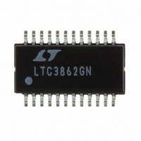
LTC3862IGN#PBF Linear Technology, LTC3862IGN#PBF Datasheet - Page 24

LTC3862IGN#PBF
Manufacturer Part Number
LTC3862IGN#PBF
Description
IC CTRLR DC/DC STPUP 24SSOP
Manufacturer
Linear Technology
Type
Step-Up (Boost)r
Datasheet
1.LTC3862EGNPBF.pdf
(40 pages)
Specifications of LTC3862IGN#PBF
Internal Switch(s)
No
Synchronous Rectifier
No
Number Of Outputs
1
Voltage - Output
1.22 ~ 200 V
Current - Output
50mA
Frequency - Switching
300kHz
Voltage - Input
4 ~ 36 V
Operating Temperature
-40°C ~ 125°C
Mounting Type
Surface Mount
Package / Case
24-SSOP
Primary Input Voltage
36V
No. Of Outputs
1
Output Current
50mA
No. Of Pins
24
Operating Temperature Range
-40°C To +125°C
Msl
MSL 1 - Unlimited
Supply Voltage Range
4V To 36V
Rohs Compliant
Yes
Lead Free Status / RoHS Status
Lead free / RoHS Compliant
Power - Output
-
LTC3862
Typical Boost Applications Circuit
A basic 2-phase, single output LTC3862 application circuit is
shown in Figure 18. External component selection is driven
by the characteristics of the load and the input supply.
Duty Cycle Considerations
For a boost converter operating in a continuous conduction
mode (CCM), the duty cycle of the main switch is:
where V
minimum on-time for a given application operating in
CCM is:
For a given input voltage range and output voltage, it is
important to know how close the minimum on-time of the
application comes to the minimum on-time of the control
IC. The LTC3862 minimum on-time can be programmed
from 180ns to 340ns using the BLANK pin.
APPLICATIONS INFORMATION
24
D
t
ON MIN
=
(
⎛
⎜
⎝
10nF
F
V
is the forward voltage of the boost diode. The
O
)
100pF
66.5k
68.1k
10nF
V
+
=
O
V
OUT
V
1
f
+
F
⎛
⎜
⎝
V
–
12.4k
V
F
O
475k
V
IN
+
⎞
⎟ =
⎠
V
V
F
O
Figure 18. A Typical 2-Phase, Single Output Boost Converter Application Circuit
–
+
D
SLOPE
BLANK
PHASEMODE
FREQ
SS
ITH
FB
SGND
CLKOUT
SYNC
PLLFLTR
t
ON
MAX
V
V
IN MAX
F
(
•
LTC3862
f
)
SENSE1
SENSE1
SENSE2
SENSE2
⎞
⎟
⎠
INTV
GATE1
GATE2
PGND
RUN
3V8
V
CC
IN
+
–
–
+
24.9k
4.7μF
1nF
1μF
10nF
10nF
84.5k
5V TO 36V
V
IN
Minimum On-Time Limitations
In a single-ended boost converter, two steady-state condi-
tions can result in operation at the minimum on-time of
the controller. The fi rst condition is when the input voltage
is close to the output voltage. When V
the voltage across the inductor approaches zero during
the switch off-time. Under this operating condition the
converter can become unstable and the output can experi-
ence high ripple voltage oscillation at audible frequencies.
For applications where the input voltage can approach
or exceed the output voltage, consider using a SEPIC or
buck-boost topology instead of a boost converter.
The second condition that can result in operation at the
minimum on-time of the controller is at light load, in deep
discontinuous mode. As the load current is decreased,
the on-time of the switch decreases, until the minimum
on-time limit of the controller is reached. Any further de-
crease in the output current will result in pulse skipping,
a typically benign condition where cycles are skipped in
order to maintain output regulation.
6.8μF 50V
10Ω
PA2020-193
PA2020-193
10Ω
19.4μH
19.4μH
6.8μF 50V
6.8μF 50V
L1
L2
0.006Ω
1W
Q1
HAT2266H
0.006Ω
1W
Q2
HAT2266H
PDS760
PDS760
D1
D2
100μF
100μF
63V
63V
+
+
6.8μF 50V
6.8μF 50V
6.8μF 50V
6.8μF 50V
IN
3862 F18
approaches V
V
48V
2A TO 5A
OUT
3862fb
OUT


