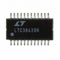
LTC3862IGN#PBF Linear Technology, LTC3862IGN#PBF Datasheet - Page 15

LTC3862IGN#PBF
Manufacturer Part Number
LTC3862IGN#PBF
Description
IC CTRLR DC/DC STPUP 24SSOP
Manufacturer
Linear Technology
Type
Step-Up (Boost)r
Datasheet
1.LTC3862EGNPBF.pdf
(40 pages)
Specifications of LTC3862IGN#PBF
Internal Switch(s)
No
Synchronous Rectifier
No
Number Of Outputs
1
Voltage - Output
1.22 ~ 200 V
Current - Output
50mA
Frequency - Switching
300kHz
Voltage - Input
4 ~ 36 V
Operating Temperature
-40°C ~ 125°C
Mounting Type
Surface Mount
Package / Case
24-SSOP
Primary Input Voltage
36V
No. Of Outputs
1
Output Current
50mA
No. Of Pins
24
Operating Temperature Range
-40°C To +125°C
Msl
MSL 1 - Unlimited
Supply Voltage Range
4V To 36V
Rohs Compliant
Yes
Lead Free Status / RoHS Status
Lead free / RoHS Compliant
Power - Output
-
Operation at High Supply Voltage
At high input voltages, the LTC3862’s internal LDO can
dissipate a signifi cant amount of power, which could
cause the maximum junction temperature to be exceeded.
Conditions such as a high operating frequency, or the use
of more than one power MOSFET per channel, could push
the junction temperature rise to high levels. If the thermal
equations above indicate too high a rise in the junction
temperature, an external bias supply can always be used
to reduce the power dissipation on the IC, as shown in
Figure 3.
For example, a 5V or 12V system rail that is available
would be more suitable than the 24V main input power
rail to power the LTC3862. Also, the bias power can be
generated with a separate switching or LDO regulator. An
example of an LDO regulator is shown in Figure 3. The
output voltage of the LDO regulator can be set by selecting
an appropriate zener diode to be higher than 5V but low
enough to divide the power dissipation between LTC3862
and Q1 in Figure 3. The absolute maximum voltage rating
of the INTV
Power Supply Sequencing
As shown in Figure 1, there are body diodes in parallel
with the PMOS output transistors in the two LDO regula-
tors in the LTC3862. As a result, it is not possible to bias
the INTV
supplies. Independently biasing the INTV
separate power supply can cause one of two possible
failure modes during supply sequencing. If the INTV
supply comes up before the V
OPERATION
Figure 3. Using the LTC3862 with an External Bias Supply
CC
CC
and V
pin is 6V.
R1
D1
IN
pins of the chip from separate power
C
VCC
(OPT)
V
IN
Q1
IN
supply, high current will
V
INTV
IN
LTC3862
CC
3862 F03
CC
pin from a
CC
fl ow from the external INTV
diode of the LDO PMOS device, to the input capacitor
and V
condition and cause catastrophic failure of the IC.
If, however, the V
INTV
load to the internal LDO in the LTC3862, and the LDO will
attempt to charge the INTV
current. This will result in excessive power dissipation and
possible thermal overload of the LTC3862.
If an independent 5V supply exists in the system, it may be
possible to short INTV
reduce gate drive power dissipation. With V
shorted together, the LDO output PMOS transistor is biased
at V
and digital control circuitry, as well as the gate drive cur-
rent, will be supplied by the external 5V supply.
Programming the Output Voltage
The output voltage is set by a resistor divider according
to the following formula:
The external resistor divider is connected to the output
as shown in Figure 4. Resistor R1 is normally chosen so
that the output voltage error caused by the current fl owing
out of the V
compared to the current in the divider. For an output volt-
age error due to the error amp input bias current of less
than 0.5%, this translates to a maximum value of R1 of
about 30k.
V
DS
OUT
CC
IN
= 0V, and the current demand of the internal analog
pin. This high current fl ow could trigger a latchup
supply, the external INTV
=
Figure 4. Programming the Output Voltage
with a Resistor Divider
1 223
.
FB
pin during normal operation is negligible
IN
V
⎛
⎝ ⎜
supply to the IC comes up before the
LTC3862
1
+
CC
SGND
R
R
and V
FB
2
1
CC
⎞
⎠ ⎟
CC
output with its short-circuit
IN
supply, through the body
together to 5V in order to
V
CC
OUT
R2
R1
3862 F04
supply will act as a
LTC3862
IN
and INTV
15
3862fb
CC


