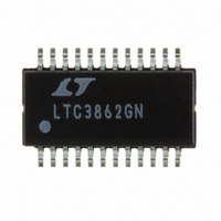
LTC3862IGN#PBF Linear Technology, LTC3862IGN#PBF Datasheet - Page 28

LTC3862IGN#PBF
Manufacturer Part Number
LTC3862IGN#PBF
Description
IC CTRLR DC/DC STPUP 24SSOP
Manufacturer
Linear Technology
Type
Step-Up (Boost)r
Datasheet
1.LTC3862EGNPBF.pdf
(40 pages)
Specifications of LTC3862IGN#PBF
Internal Switch(s)
No
Synchronous Rectifier
No
Number Of Outputs
1
Voltage - Output
1.22 ~ 200 V
Current - Output
50mA
Frequency - Switching
300kHz
Voltage - Input
4 ~ 36 V
Operating Temperature
-40°C ~ 125°C
Mounting Type
Surface Mount
Package / Case
24-SSOP
Primary Input Voltage
36V
No. Of Outputs
1
Output Current
50mA
No. Of Pins
24
Operating Temperature Range
-40°C To +125°C
Msl
MSL 1 - Unlimited
Supply Voltage Range
4V To 36V
Rohs Compliant
Yes
Lead Free Status / RoHS Status
Lead free / RoHS Compliant
Power - Output
-
LTC3862
APPLICATIONS INFORMATION
For a boost converter where the current limit value is
chosen to be 30% higher than the maximum load current,
the peak current in the MOSFET and sense resistor is:
The sense resistor value is then:
Again, the factor n is the number of phases used, and χ
represents the percentage ripple current in the inductor.
The number 1.3 represents the factor by which the cur-
rent limit exceeds the maximum load current, I
For example, if the current limit needs to exceed the
maximum load current by 50%, then the 1.3 factor should
be replaced with 1.5.
The average power dissipated in the sense resistor can
easily be calculated as:
This equation assumes no temperature coeffi cient for
the sense resistor. If the resistor chosen has a signifi cant
temperature coeffi cient, then substitute the worst-case
high resistance value into the equation.
28
I
R
P
SW MAX
R SENSE
SENSE
(
(
)
=
)
=
=
V
I
SENSE MAX
R SENSE
⎛
⎜
⎝
(
1 3
n
1 3
. •
• –
. •
(
(
1
⎛
⎝ ⎜
I
)
1
O MAX
D
=
+
(
)
MAX
n
1
• • –
χ
2
n
⎞
⎠ ⎟
•
)
⎛
⎝ ⎜
)
• •
(
⎞
⎟
⎠
1
I
1
O MAX
2
+
(
•
χ
INDUCTOR
2
D
SW NODE
CURRENT
CURRENT
R
10V/DIV
⎞
⎠ ⎟
MAX
SEN
2A/DIV
2A/DIV
DIODE
)
•
1 3
S S E
)
. •
Figure 21. Diode Current Waveform for a
High Duty Cycle Application
– 1 D
V
V
IN
OUT
•
= 6V
D
I
O MAX
= 24V
MAX
MAX
(
O(MAX)
) )
.
1μs/DIV
The resistor temperature can be calculated using the
equation:
Selecting the Output Diodes
To maximize effi ciency, a fast switching diode with low
forward drop and low reverse leakage is required. The
output diode in a boost converter conducts current during
the switch off-time. The peak reverse voltage that the diode
must withstand is equal to the regulator output voltage.
The average forward current in normal operation is equal
to the output current, and the peak current is equal to the
peak inductor current:
Although the average diode current is equal to the output
current, in very high duty cycle applications (low V
high V
higher than the average, as shown in Figure 21. In this
case check the diode manufacturer’s data sheet to ensure
that its peak current rating exceeds the peak current in
the equation above. In addition, when calculating the
power dissipation in the diode, use the value of the
forward voltage (V
the average output current. Excess power will be dissi-
pated in the series resistance of the diode, which would
not be accounted for if the average output current and
forward voltage were used in the equations. Finally, this
T
I
D PEAK
D
(
= T
OUT
A
) the peak diode current can be several times
)
+ P
=
3862 F21
n
1
R(SENSE)
•
⎛
⎝ ⎜
1
F
+
) measured at the peak current, not
χ
2
• R
⎞
⎠ ⎟
•
TH(JA)
1
I
O MAX
–
(
D
MAX
)
IN
3862fb
to


