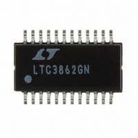
LTC3862IGN#PBF Linear Technology, LTC3862IGN#PBF Datasheet - Page 17

LTC3862IGN#PBF
Manufacturer Part Number
LTC3862IGN#PBF
Description
IC CTRLR DC/DC STPUP 24SSOP
Manufacturer
Linear Technology
Type
Step-Up (Boost)r
Datasheet
1.LTC3862EGNPBF.pdf
(40 pages)
Specifications of LTC3862IGN#PBF
Internal Switch(s)
No
Synchronous Rectifier
No
Number Of Outputs
1
Voltage - Output
1.22 ~ 200 V
Current - Output
50mA
Frequency - Switching
300kHz
Voltage - Input
4 ~ 36 V
Operating Temperature
-40°C ~ 125°C
Mounting Type
Surface Mount
Package / Case
24-SSOP
Primary Input Voltage
36V
No. Of Outputs
1
Output Current
50mA
No. Of Pins
24
Operating Temperature Range
-40°C To +125°C
Msl
MSL 1 - Unlimited
Supply Voltage Range
4V To 36V
Rohs Compliant
Yes
Lead Free Status / RoHS Status
Lead free / RoHS Compliant
Power - Output
-
The LTC3862 uses a constant frequency architecture that
can be programmed over a 75kHz to 500kHz range using
a single resistor from the FREQ pin to ground. Figure 6
illustrates the relationship between the FREQ pin resistance
and the operating frequency.
The operating frequency of the LTC3862 can be approxi-
mated using the following formula:
A phase-lock loop is available on the LTC3862 to syn-
chronize the internal oscillator to an external clock source
connected to the SYNC pin. Connect a series RC network
from the PLLFLTR pin to SGND to compensate PLL’s
feedback loop. Typical compensation components are a
0.01μF capacitor in series with a 10k resistor. The PLLFLTR
pin is both the output of the phase detector and the input
to the voltage controlled oscillator (VCO). The LTC3862
phase detector adjusts the voltage on the PLLFLTR pin
to align the rising edge of GATE1 to the leading edge of
the external clock signal, as shown in Figure 7. The ris-
ing edge of GATE2 will depend upon the voltage on the
PHASEMODE pin. The capture range of the LTC3862’s PLL
is 50kHz to 650kHz.
Because the operating frequency of the LTC3862 can be
programmed using an external resistor, in synchronized
applications, it is recommended that the free-running fre-
quency (as defi ned by the external resistor) be set to the
same value as the synchronized frequency. This results in
a start-up of the IC at approximately the same frequency
as the external clock, so that when the sync signal comes
alive, no discontinuity at the output will be observed. It also
ensures that the operating frequency remains essentially
constant in the event the sync signal is lost. The SYNC
pin has an internal 50k resistor to ground.
Using the CLKOUT and PHASEMODE Pins
in Multi-Phase Applications
The LTC3862 features two pins (CLKOUT and PHASEMODE)
that allow multiple ICs to be daisy-chained together for
higher current multi-phase applications. For a 3- or 4-phase
OPERATION
R
FREQ
= 5.5096E9(f
OSC
)
–0.9255
design, the CLKOUT signal of the master controller is con-
nected to the SYNC input of the slave controller in order
to synchronize additional power stages for a single high
current output. The PHASEMODE pin is used to adjust the
phase relationship between channel 1 and channel 2, as well
as the phase relationship between channel 1 and CLKOUT,
as summarized in Table 1. The phases are calculated rela-
tive to the zero degrees, defi ned as the rising edge of the
GATE1 output. In a 6-phase application the CLKOUT pin
of the master controller connects to the SYNC input of the
2nd controller and the CLKOUT pin of the 2nd controller
connects to the SYNC pin of the 3rd controller.
10V/DIV
10V/DIV
10V/DIV
CLKOUT
10V/DIV
GATE1
GATE2
SYNC
Figure 6. FREQ Pin Resistor Value vs Frequency
1000
Figure 7. Synchronization of the LTC3862
to an External Clock Using the PLL
100
V
V
PHASEMODE = SGND
10
IN
OUT
0
= 12V
= 48V 1A
100
200
300
FREQUENCY (kHz)
400
2μs/DIV
500
600
700
800
900
LTC3862
3862 F06
1000
3862 F07
17
3862fb


