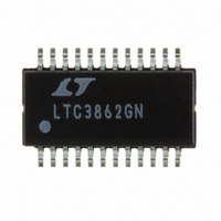
LTC3862IGN#PBF Linear Technology, LTC3862IGN#PBF Datasheet - Page 21

LTC3862IGN#PBF
Manufacturer Part Number
LTC3862IGN#PBF
Description
IC CTRLR DC/DC STPUP 24SSOP
Manufacturer
Linear Technology
Type
Step-Up (Boost)r
Datasheet
1.LTC3862EGNPBF.pdf
(40 pages)
Specifications of LTC3862IGN#PBF
Internal Switch(s)
No
Synchronous Rectifier
No
Number Of Outputs
1
Voltage - Output
1.22 ~ 200 V
Current - Output
50mA
Frequency - Switching
300kHz
Voltage - Input
4 ~ 36 V
Operating Temperature
-40°C ~ 125°C
Mounting Type
Surface Mount
Package / Case
24-SSOP
Primary Input Voltage
36V
No. Of Outputs
1
Output Current
50mA
No. Of Pins
24
Operating Temperature Range
-40°C To +125°C
Msl
MSL 1 - Unlimited
Supply Voltage Range
4V To 36V
Rohs Compliant
Yes
Lead Free Status / RoHS Status
Lead free / RoHS Compliant
Power - Output
-
In order to satisfy these different applications require-
ments, the LTC3862 has a simple way to program the
maximum duty cycle. Connecting the D
limits the maximum duty cycle to 96%. Floating this pin
limits the duty cycle to 84% and connecting the D
to the 3V8 supply limits it to 75%. Figure 14 illustrates
the effect of limiting the maximum duty cycle on the SW
node waveform of a boost converter.
OPERATION
INDUCTOR
INDUCTOR
INDUCTOR
CURRENT
CURRENT
CURRENT
SW NODE
SW NODE
SW NODE
20V/DIV
20V/DIV
20V/DIV
1A/DIV
2V/DIV
1A/DIV
2V/DIV
1A/DIV
2V/DIV
GATE
GATE
GATE
MINIMUM ON-TIME AT LIGHT LOAD WITH BLANK = FLOAT
MINIMUM ON-TIME AT LIGHT LOAD WITH BLANK = SGND
Figure 13. Leading Edge Blanking Effects
on the Minimum On-Time
MINIMUM ON-TIME AT LIGHT LOAD WITH BLANK = 3V8
V
V
MEASURED ON-TIME = 180ns
V
V
MEASURED ON-TIME = 260ns
V
V
MEASURED ON-TIME = 340ns
IN
OUT
IN
OUT
IN
OUT
= 30V
= 30V
= 30V
= 48V
= 48V
= 48V
200ns/DIV
200ns/DIV
200ns/DIV
MAX
3862 F13
pin to SGND
MAX
pin
The LTC3862 contains an oscillator that runs at a multiple
of the switching frequency, in order to provide for 2-, 3-,
4-, 6- and 12-phase operation. A digital counter is used
to divide down the fundamental oscillator frequency in
order to obtain the operating frequency of the gate drivers.
Since the maximum duty cycle limit is obtained from this
digital counter, the percentage maximum duty cycle does
not vary with process tolerances or temperature.
Figure 14. SW Node Waveforms with Different Duty Cycle Limits
INDUCTOR
INDUCTOR
INDUCTOR
SW NODE
CURRENT
SW NODE
CURRENT
SW NODE
CURRENT
10V/DIV
10V/DIV
10V/DIV
2A/DIV
2A/DIV
2A/DIV
96% MAXIMUM DUTY CYCLE WITH D
84% MAXIMUM DUTY CYCLE WITH D
75% MAXIMUM DUTY CYCLE WITH D
1μs/DIV
1μs/DIV
1μs/DIV
MAX
MAX
MAX
LTC3862
= SGND
= FLOAT
= 3V8
3862 F14
21
3862fb


