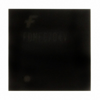
FDMF8704V Fairchild Semiconductor, FDMF8704V Datasheet - Page 3

FDMF8704V
Manufacturer Part Number
FDMF8704V
Description
IC MOD DVR/FET W/VREG 56MLP 8X8
Manufacturer
Fairchild Semiconductor
Type
Step-Down (Buck)r
Datasheet
1.FDMF8704V.pdf
(11 pages)
Specifications of FDMF8704V
Internal Switch(s)
Yes
Synchronous Rectifier
Yes
Number Of Outputs
1
Voltage - Output
0.8 ~ 3.2 V
Current - Output
32A
Frequency - Switching
1MHz
Voltage - Input
7 ~ 20 V
Operating Temperature
-55°C ~ 150°C
Mounting Type
Surface Mount
Package / Case
56-MLP
Power - Output
10W
Supply Voltage (min)
4.5 V
Supply Current
50 mA
Maximum Operating Temperature
+ 150 C
Mounting Style
SMD/SMT
Minimum Operating Temperature
- 55 C
Number Of Drivers
1
Lead Free Status / RoHS Status
Lead free / RoHS Compliant
Other names
FDMF8704VTR
FDMF8704V Rev. G
Absolute Maximum Rating
Stresses exceeding the absolute maximum ratings may damage the device. The device may not function or be operable above the
recommended operating conditions and stressing the parts to these levels is not recommended. In addition, extended exposure to
stresses above the recommended operating conditions may affect device reliability. The absolute maximum ratings are stress ratings
only.
Note 1: Package power dissipation based on 4 layers, 2 square inch, 2 oz. copper pad. R
Recommended Operating Range
The Recommended Operating Conditions table defines the conditions for actual device operation. Recommended operating condi-
tions are specified to ensure optimal performance to the datasheet specifications. Fairchild does not recommend exceeding them or
designing to Absolute Maximum Ratings.
Electrical Characteristics
V
Note 2: t
Parameter
V
V
BOOT to VSWH
VAUX to PGND
VSWH to PGND
BOOT to PGND
I
I
R
P
Operating and Storage Junction Temperature Range
Parameter
V
V
V
Parameter
Operating Voltage Range
Control Circuit Supply Current
PWM Input High Voltage
PWM Input Low Voltage
PWM Input Current
DISB Input High Voltage
DISB Input Low Voltage
DISB Input Current
Auxiliary Input Voltage Operating Range V
Regulator Output Voltage
Propagation Delay
O(AV)
O(PK)
IN
CIN
IN
D
CIN
IN
OUT
θJPCB
= 12V, V
to PGND
, PWM, DISB to PGND
thermal resistance with PCB temperature referenced at VSWH pin.
PDL(LDRV/HRDV)
CIN
= 5V, T
Control Circuit Supply Voltage
Output Stage Supply Voltage
Output Voltage
V
V
Junction to PCB Thermal Resistance (note 1)
T
PCB
IN
IN
A
refers to HIGH-to-LOW transition, t
= 12V, V
= 12V, t
= 25°C unless otherwise noted.
= 100°C (note 1)
PULSE
O
= 1.3V, f
= 10µs
V
I
V
V
I
V
V
I
V
t
t
t
t
t
t
CC
IL(PWM)
DISB
PDL(DISB-LDRV)
PDH(DISB-LDRV)
PDL(LDRV)
PDL(HDRV)
PDH(LDRV)
PDH(HDRV)
sw
AUX
CC
IH(PWM)
IL(PWM)
IHDISB)
IL(DISB)
REGOUT
Symbol
= 1MHz, T
(2)
(2)
(2)
(2)
PCB
(2)
(2)
PDH(LDRV/HDRV)
= 100°C
f
f
V
f
SW
SW
sw
IN
3
= 1MHz, I
= 12V, V
= 0Hz, V
= 1MHz, V
Conditions
Min.
OUT
DISB
4.5
0.8
O
refers to LOW-to-HIGH transition.
7
DISB
= 30A
= 1.3V,
= 5V
= 5V
Min.
-0.3
-0.3
-0.3
-0.3
-1.0
-0.3
-55
θJPCB
Typ.
1.3
12
5
Min.
is the steady state junction to PCB
4.75
4.5
2.4
2.4
-2
-2
7
Max.
150
24
20
24
30
32
65
10
6
6
5
Max.
Typ.
5.5
3.2
50
22
12
20
20
5
1
5
8
6
9
Max. Units
5.25
5.5
0.8
0.8
20
3
2
2
www.fairchildsemi.com
Units
°C/W
Units
°C
W
V
V
V
V
V
A
A
V
V
V
V
mA
µA
µA
ns
ns
ns
ns
ns
ns
V
V
V
V
V
V
V


