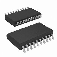
ISL6755AAZA-T Intersil, ISL6755AAZA-T Datasheet - Page 15

ISL6755AAZA-T
Manufacturer Part Number
ISL6755AAZA-T
Description
IC CTRLR PWM FULL-BRDG 20-QSOP
Manufacturer
Intersil
Datasheet
1.ISL6755AAZA.pdf
(17 pages)
Specifications of ISL6755AAZA-T
Pwm Type
Voltage/Current Mode
Number Of Outputs
4
Frequency - Max
2MHz
Duty Cycle
100%
Voltage - Supply
9 V ~ 16 V
Buck
No
Boost
No
Flyback
No
Inverting
No
Doubler
No
Divider
No
Cuk
No
Isolated
No
Operating Temperature
-40°C ~ 105°C
Package / Case
20-QSOP
Frequency-max
2MHz
Lead Free Status / RoHS Status
Lead free / RoHS Compliant
This condition persists through the remainder of the
half-cycle.
During the period when CT discharges, also referred to as
the deadtime, the upper switches toggle. Switch UL turns off
and switch UR turns on. The actual timing of the upper
switch toggle is dependent on RESDEL which sets the
resonant delay. The voltage applied to RESDEL determines
how far in advance the toggle occurs prior to a lower switch
turning on. The ZVS transition occurs after the upper
switches toggle and before the diagonal lower switch turns
on. The required resonant delay is 1/4 of the period of the LC
resonant frequency of the circuit formed by the leakage
inductance and the parasitic capacitance. The resonant
transition may be estimated from Equation 28.
where τ is the resonant transition time, L
inductance, C
equivalent resistance in series with L
The resonant delay is always less than or equal to the
deadtime and may be calculated using Equation 29.
where τ
voltage between 0 and 2V applied to the RESDEL pin, and
DT is the deadtime (see Equations 1 through 5).
When the upper switches toggle, the primary current that
was flowing through UL must find an alternate path. It
charges/discharges the parasitic capacitance of switches UL
and LL until the body diode of LL is forward biased. If
RESDEL is set properly, switch LL will be turned on at this
time.The output inductor does not assist this transition. It is
purely a resonant transition driven by the leakage
inductance.
τ
τ
VIN+
resdel
VIN-
FIGURE 16. UPPER SWITCH TOGGLE AND RESONANT
=
π
-- -
2
UL
-----------------------------------
LL
-------------- -
L
=
resdel
L
1
C
V
------------------- - DT
P
1
resdel
I
P
–
2
TRANSITION
P
is the desired resonant delay, V
--------- -
4L
R
is the parasitic capacitance, and R is the
2
2
L
⋅
UR
LR
L
L
S
15
D1
D2
L
and C
L
I
is the leakage
S
P
resdel
.
is a
(EQ. 28)
(EQ. 29)
VOUT+
RTN
ISL6755
The second power transfer period commences when switch
LL closes. With switches UR and LL on, the primary and
secondary currents flow as indicated in Figure 17.
The UR - LL power transfer period terminates when switch
LL turns off as determined by the PWM. The current flowing
in the primary must find an alternate path. The current flows
into the parasitic switch capacitance which charges the node
to V
switch UL. As before, the output inductor current assists in
this transition. The primary leakage inductance, L
maintains the current, which now circulates around the path
of switch UR, the transformer primary, and switch UL. When
switch LL opens, the output inductor current free-wheels
predominantly through diode D1. Diode D2 may actually
conduct very little or none of the free-wheeling current,
depending on circuit parasitics. This condition persists
through the remainder of the half-cycle.
When the upper switches toggle, the primary current that
was flowing through UR must find an alternate path. It
charges/discharges the parasitic capacitance of switches UR
and LR until the body diode of LR is forward biased. If
RESDEL is set properly, switch LR will be turned on at this
time.
VIN+
VIN-
VIN+
VIN-
IN
UL
LL
UL
LL
and then forward biases the body diode of upper
FIGURE 18. UR - UL FREE-WHEELING PERIOD
FIGURE 17. UR - LL POWER TRANSFER
I
P
UR
LR
UR
LR
L
L
L
L
D1
D2
D1
D2
I
S
September 29, 2008
L
,
FN6442.1
VOUT+
VOUT+
RTN
RTN


