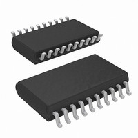
ISL6755AAZA-T Intersil, ISL6755AAZA-T Datasheet

ISL6755AAZA-T
Specifications of ISL6755AAZA-T
Related parts for ISL6755AAZA-T
ISL6755AAZA-T Summary of contents
Page 1
... PART RANGE (Note) MARKING (°C) ISL6755AAZA* 6755 AAZ -40 to +105 20 Ld QSOP M20.15 *Add -T suffix to part number for tape and reel packaging NOTE: These Intersil Pb-free plastic packaged products employ special Pb-free material sets, molding compounds/die attach materials, and 100% matte tin plate plus anneal (e3 termination finish, which is RoHS compliant and compatible with both SnPb and Pb-free soldering operations) ...
Page 2
Functional Block Diagram VDD VREF UVLO OVER- TEMPERATURE PROTECTION GND VREF RESDEL IOUT 4X OSCILLATOR CT RTD CTBUF SS 50% PWM STEERING LOGIC PWM SAMPLE + AND HOLD - 1.00V OVER CURRENT COMPARATOR PWM COMPARATOR 80mV VREF + - 0.33 ...
Page 3
Typical Application - High Voltage Input ZVS Full-Bridge Converter VIN+ CR2 R19 Q8A Q8B 400 VDC Q6A Q6B Q4 VIN- T2 CR1 R10 VDD BIAS CR3 T3 Q2 R20 Q5A ...
Page 4
... ISL6755 Thermal Information Thermal Resistance (Typical) 20 Lead QSOP (Note 1 0.3V REF Maximum Junction Temperature . . . . . . . . . . . . . . .-55°C to +150°C Maximum Storage Temperature Range . . . . . . . . . .-65°C to +150°C Pb-Free Reflow Profile .see link below http://www.intersil.com/pbfree/Pb-FreeReflow.asp < 20V, RTD = 10.0kΩ 470pF TEST CONDITIONS LOAD ...
Page 5
Electrical Specifications Recommended operating conditions unless otherwise noted. Refer to Block Diagram and Typical Application schematic. 9V < +25°C; Parameters with MIN and/or MAX limits are 100% tested at +25°C, unless otherwise specified. A Temperature limits established ...
Page 6
Electrical Specifications Recommended operating conditions unless otherwise noted. Refer to Block Diagram and Typical Application schematic. 9V < +25°C; Parameters with MIN and/or MAX limits are 100% tested at +25°C, unless otherwise specified. A Temperature limits established ...
Page 7
Typical Performance Curves 1.02 1.01 1 0.99 0.98 -40 -25 - TEMPERATURE (¬¨Ð FIGURE 1. REFERENCE VOLTAGE vs TEMPERATURE 4 1- 1000pF CT = 1000pF CT = 680pF CT = 680pF CT = 470pF CT ...
Page 8
RC network to produce the desired sawtooth waveform. OUTUL and OUTUR - These outputs control the upper bridge FETs and operate at a fixed 50% duty cycle in alternate sequence. OUTUL controls the upper left FET and OUTUR ...
Page 9
The maximum duty cycle, D, and percent deadtime, DT, can be calculated from ----------- - – Soft-Start Operation The ISL6755 features a soft-start using an external capacitor in conjunction with ...
Page 10
CHANNEL 1 (YELLOW): OUTLL CHANNEL 2 (RED): OUTLR CHANNEL 3 (BLUE): CS CHANNEL 4 (GREEN): IOUT FIGURE 6. DYNAMIC BEHAVIOR IOUT The average current signal on I remains accurate OUT provided that the output inductor current is ...
Page 11
The peak overcurrent behavior is similar to most other PWM controllers. If the peak current exceeds 1.0V, the active output pulse is terminated immediately. If voltage-mode control is used in a bridge topology, it should be noted that peak current ...
Page 12
Adding the external ramp to the current feedback signal is the more popular method. From the small signal current-mode model [1] it can be shown that the naturally-sampled modulator gain, Fm, without slope compensation ...
Page 13
CS pin as shown in Figure 10 FIGURE 10. ADDING SLOPE COMPENSATION Assuming the designer has selected values for the RC ...
Page 14
Equation 24 becomes: ( Δ ⋅ – Ω ------------------------------------------------------------ - R9 = ΔV V – The buffer transistor used to create the external ramp from CT should have a sufficiently ...
Page 15
This condition persists through the remainder of the half-cycle. During the period when CT discharges, also referred to as the deadtime, the upper switches toggle. Switch UL turns off and switch UR turns on. The actual timing of the upper ...
Page 16
VIN VIN- FIGURE 19. UPPER SWITCH TOGGLE AND RESONANT TRANSITION The first power transfer period commences when switch LR closes and the cycle repeats. The ZVS transition requires that the ...
Page 17
... Accordingly, the reader is cautioned to verify that data sheets are current before placing orders. Information furnished by Intersil is believed to be accurate and reliable. However, no responsibility is assumed by Intersil or its subsidiaries for its use; nor for any infringements of patents or other rights of third parties which may result from its use ...


