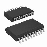
ISL6755AAZA-T Intersil, ISL6755AAZA-T Datasheet - Page 13

ISL6755AAZA-T
Manufacturer Part Number
ISL6755AAZA-T
Description
IC CTRLR PWM FULL-BRDG 20-QSOP
Manufacturer
Intersil
Datasheet
1.ISL6755AAZA.pdf
(17 pages)
Specifications of ISL6755AAZA-T
Pwm Type
Voltage/Current Mode
Number Of Outputs
4
Frequency - Max
2MHz
Duty Cycle
100%
Voltage - Supply
9 V ~ 16 V
Buck
No
Boost
No
Flyback
No
Inverting
No
Doubler
No
Divider
No
Cuk
No
Isolated
No
Operating Temperature
-40°C ~ 105°C
Package / Case
20-QSOP
Frequency-max
2MHz
Lead Free Status / RoHS Status
Lead free / RoHS Compliant
sums this signal with the current sense feedback and applies
the result to the CS pin as shown in Figure 10.
Assuming the designer has selected values for the RC filter
placed on the CS pin, the value of R9 required to add the
appropriate external ramp can be found by superposition.
Rearranging to solve for R9 yields
The value of R
rescaled so that the current sense signal presented at the
CS pin is that predicted by Equation 17. The divider created
by R6 and R9 makes this necessary.
Example:
V
V
L
Np/Ns = 20
Lm = 2mH
I
Oscillator Frequency, Fsw = 400kHz
Duty Cycle, D = 85.7%
N
R6 = 499Ω
R9
R′
V
O
O
IN
O
CT
e
CS
= 55A
–
= 2.0μH
= 12V
=
= 280V
ΔV
= 50
=
(
------------------------------------------------------------------------------------------------------------------ -
D V
CS
R6
--------------------- - R
(
FIGURE 10. ADDING SLOPE COMPENSATION
R9
CTBUF
=
+
R9
(
------------------------------------------------------------------------------ -
D V
CS
(
⋅
–
CTBUF
determined in Equation 19 or 22 must be
CS
0.4
V
e
) V
R6
–
–
R
CS
–
ΔV
+
e
0.4
R6
+
R9
CS
13
ΔV
)
R9
+
CS
0.4
) R6
+
C4
⋅
0.4
10
1
2
3
4
5
6
7
8
9
) R6
CTBUF
RAMP
CS
⋅
ISL6755
V
Ω
GND
GND
(EQ. 23)
(EQ. 24)
(EQ. 25)
20
19
18
17
16
15
14
13
12
11
ISL6755
Solve for the current sense resistor, R
R
Determine the amount of voltage, Ve, that must be added to
the current feedback signal using Equation 16.
Ve = 153mV
Next, determine the effect of the magnetizing current from
Equation 21.
ΔV
Using Equation 24, solve for the summing resistor, R9, from
CTBUF to CS.
R9 = 30.1kΩ
Determine the new value of R
R’
The above discussion determines the minimum external
ramp that is required. Additional slope compensation may be
considered for design margin.
If the application requires deadtime less than about 500ns,
the CTBUF signal may not perform adequately for slope
compensation. CTBUF lags the CT sawtooth waveform by
300ns to 400ns. This behavior results in a non-zero value of
CTBUF when the next half-cycle begins when the deadtime
is short.
Under these situations, slope compensation may be added
by externally buffering the CT signal as shown below.
Using CT to provide slope compensation instead of CTBUF
requires the same calculations, except that Equations 23
and 24 require modification. Equation 23 becomes:
V
CS
e
CS
CS
FIGURE 11. ADDING SLOPE COMPENSATION USING CT
–
ΔV
= 15.1Ω.
= 15.4Ω
= 91mV
CS
=
--------------------- -
R6
2D R6
R
+
CS
⋅
R9
R9
C4
R6
V
CS
, R’
CS
CS
, using Equation 25.
, using Equation 19.
10
CT
1
2
3
4
5
6
7
8
9
CT
RAMP
CS
ISL6755
September 29, 2008
VREF
GND
GND
(EQ. 26)
FN6442.1
20
19
16
15
14
13
12
11
18
17


