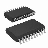
ISL6755AAZA-T Intersil, ISL6755AAZA-T Datasheet - Page 14

ISL6755AAZA-T
Manufacturer Part Number
ISL6755AAZA-T
Description
IC CTRLR PWM FULL-BRDG 20-QSOP
Manufacturer
Intersil
Datasheet
1.ISL6755AAZA.pdf
(17 pages)
Specifications of ISL6755AAZA-T
Pwm Type
Voltage/Current Mode
Number Of Outputs
4
Frequency - Max
2MHz
Duty Cycle
100%
Voltage - Supply
9 V ~ 16 V
Buck
No
Boost
No
Flyback
No
Inverting
No
Doubler
No
Divider
No
Cuk
No
Isolated
No
Operating Temperature
-40°C ~ 105°C
Package / Case
20-QSOP
Frequency-max
2MHz
Lead Free Status / RoHS Status
Lead free / RoHS Compliant
and Equation 24 becomes:
The buffer transistor used to create the external ramp from
CT should have a sufficiently high gain so as to minimize the
required base current. Whatever base current is required
reduces the charging current into CT and will reduce the
oscillator frequency.
ZVS Full-Bridge Operation
The ISL6755 is a full-bridge zero-voltage switching (ZVS)
PWM controller that behaves much like a traditional
hard-switched topology controller. Rather than drive the
diagonal bridge switches simultaneously, the upper switches
(OUTUL, OUTUR) are driven at a fixed 50% duty cycle and
the lower switches (OUTLL, OUTLR) are pulse width
modulated on the trailing edge.
To understand how the ZVS method operates one must
include the parasitic elements of the circuit and examine a
full switching cycle.
In Figure 13, the power semiconductor switches have been
replaced by ideal switch elements with parallel diodes and
capacitance, the output rectifiers are ideal, and the
transformer leakage inductance has been included as a
discrete element. The parasitic capacitance has been
R9
VIN+
VIN-
DEADTIME
=
OUTUR
OUTLR
OUTUL
OUTLL
UL
LL
(
------------------------------------------------------------ -
2D V
CT
FIGURE 12. BRIDGE DRIVE SIGNAL TIMING
–
V
FIGURE 13. IDEALIZED FULL-BRIDGE
e
e
–
+
ΔV
ΔV
PWM
CS
CS
UR
LR
) R6
⋅
L
L
WINDOW
RESDEL
PWM
14
Ω
D1
D2
RESONANT
DELAY
PWM
(EQ. 27)
PWM
VOUT+
RTN
ISL6755
lumped together as switch capacitance, but represents all
parasitic capacitance in the circuit including winding
capacitance. Each switch is designated by its position, upper
left (UL), upper right (UR), lower left (LL), and lower right
(LR). The beginning of the cycle, shown in Figure 14, is
arbitrarily set as having switches UL and LR on and UR and
LL off. The direction of the primary and secondary currents
are indicated by I
The UL - LR power transfer period terminates when switch
LR turns off as determined by the PWM. The current flowing
in the primary cannot be interrupted instantaneously, so it
must find an alternate path. The current flows into the
parasitic switch capacitance of LR and UR which charges
the node to VIN and then forward biases the body diode of
upper switch UR.
The primary leakage inductance, L
which now circulates around the path of switch UL, the
transformer primary, and switch UR. When switch LR opens,
the output inductor current free-wheels through both output
diodes, D1 and D2. During the switch transition, the output
inductor current assists the leakage inductance in charging
the upper and lower bridge FET capacitance.
The current flow from the previous power transfer cycle
tends to be maintained during the free-wheeling period
because the transformer primary winding is essentially
shorted. Diode D1 may conduct very little or none of the
free-wheeling current, depending on circuit parasitics. This
behavior is quite different than occurs in a conventional
hard-switched full-bridge topology where the free-wheeling
current splits nearly evenly between the output diodes, and
flows not at all in the primary.
VIN+
VIN+
VIN-
VIN-
UL
UL
LL
LL
FIGURE 14. UL - LR POWER TRANSFER CYCLE
FIGURE 15. UL - UR FREE-WHEELING PERIOD
I
I
P
P
P
and I
UR
LR
UR
LR
L
L
S
L
L
, respectively.
D1
D2
D1
D2
L
, maintains the current
I
I
S
S
September 29, 2008
FN6442.1
VOUT+
VOUT+
RTN
RTN


