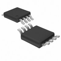
LTC1966CMS8#TRPBF Linear Technology, LTC1966CMS8#TRPBF Datasheet - Page 8

LTC1966CMS8#TRPBF
Manufacturer Part Number
LTC1966CMS8#TRPBF
Description
IC PREC RMS/DC CONV MCRPWR 8MSOP
Manufacturer
Linear Technology
Specifications of LTC1966CMS8#TRPBF
Current - Supply
155µA
Voltage - Supply
2.7 V ~ 5.5 V
Mounting Type
Surface Mount
Package / Case
8-MSOP, Micro8™, 8-uMAX, 8-uSOP,
Lead Free Status / RoHS Status
Lead free / RoHS Compliant
Available stocks
Company
Part Number
Manufacturer
Quantity
Price
pin FuncTions
LTC1966
GND (Pin 1): Ground. A power return pin.
IN1 (Pin 2): Differential Input. DC coupled (polarity is
irrelevant).
IN2 (Pin 3): Differential Input. DC coupled (polarity is
irrelevant).
V
V
The RMS averaging is accomplished with a single shunt
capacitor from this node to OUT RTN. The transfer func-
tion is given by:
8
SS
OUT
(
(Pin 4): Negative Voltage Supply. GND to – 5.5V.
V
(Pin 5): Output Voltage. This is high impedance.
OUT
–
OUT RTN
)
=
Average IN
(
2
–
IN
1
)
2
OUT RTN (Pin 6): Output Return. The output voltage is
created relative to this pin. The V
are not balanced and this pin should be tied to a low
impedance, both AC and DC. Although it is typically tied
to GND, it can be tied to any arbitrary voltage, V
RTN < (V
OUT RTN = GND.
V
ENABLE (Pin 8): An Active Low Enable Input. LTC1966
is debiased if open circuited or driven to V
operation, pull to GND, a logic low or even V
DD
(Pin 7): Positive Voltage Supply. 2.7V to 5.5V.
DD
– Max Output). Best results are obtained when
OUT
and OUT RTN pins
DD
. For normal
SS
.
SS
< OUT
1966fb


