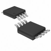
LTC1966CMS8#TRPBF Linear Technology, LTC1966CMS8#TRPBF Datasheet - Page 27

LTC1966CMS8#TRPBF
Manufacturer Part Number
LTC1966CMS8#TRPBF
Description
IC PREC RMS/DC CONV MCRPWR 8MSOP
Manufacturer
Linear Technology
Specifications of LTC1966CMS8#TRPBF
Current - Supply
155µA
Voltage - Supply
2.7 V ~ 5.5 V
Mounting Type
Surface Mount
Package / Case
8-MSOP, Micro8™, 8-uMAX, 8-uSOP,
Lead Free Status / RoHS Status
Lead free / RoHS Compliant
Available stocks
Company
Part Number
Manufacturer
Quantity
Price
applicaTions inForMaTion
However, resistive loading is an issue and the 10MΩ
impedance of a DMM or 10× scope probe will drag the
output down by –0.85% typ.
During shutdown, the switching action is halted and a
fixed 30k resistor shunts V
is discharged.
Guard Ringing the Output
The LTC1966’s combination of precision and high output
impedance can present challenges that make the use of
a guard ring around the output a good idea for many ap-
plications.
As mentioned above, a 10M resistive loading to ground
will drag down the gain far more than the specificed gain
tolerance. On a printed circuit board, contaminants from
solder flux residue to finger grime can create parasitic
resistances, which may be very high impedance, but can
have deleterious effects on the realized accuracy. As an
example, if the output (Pin 5) is routed near V
in a ±5V application, a parasitic resistance of 1G (1,000M)
is enough to introduce a –425µV output offset error, more
than the specified limit of the LTC1966 itself.
Figure 24a. PCB Layout of Figure 13 with Guard Ring
LTC1966
MS8
C
AVE
1µF
0.1µF
OUT
0.1µF
to OUT RTN so that C
1966 F24a
LT1880
SO8
SS
(Pin 4)
AVE
Use of a guard ring, wherein the LTC1966 output node is
completely surrounded by a low impedance voltage, can
reduce leakage related errors substantially. The ground
ring can be tied to OUTRTN (Pin 6) and should encircle the
output (Pin 5), the averaging capacitor terminal, and the
destination terminal at the ADC, filter op amp, or whatever
else may be next.
Figure 24a shows a sample PCB layout for the circuit of
Figure 13, wherein the guard ring trace encloses R1, R2,
and the terminals of C1, C2, and the op amp input con-
nected to the high impedance LTC1966 Output. For the
circuit of figure 14, the guard ring should enclose R1 and
the terminals of C1 and C2, as well as the terminal at the
ultimate destination.
Figure 24b shows a sample PCB layout for the circuit of
Figure 23. The summing node of the LT1494 has the same
high impedance and high accuracy as the LTC1966 output,
so here the guard ring encircles both of them. Any leakage
between them is benign because the LT1494 forces them
to the same nominal voltage.
Figure 24b. PCB Layout of Figure 23 with Guard Ring
LTC1966
MS8
C
AVE
1µF
LTC1966
LT1494
SO8
1966 F24b
27
1966fb


