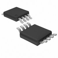
LTC1966CMS8#TRPBF Linear Technology, LTC1966CMS8#TRPBF Datasheet - Page 17

LTC1966CMS8#TRPBF
Manufacturer Part Number
LTC1966CMS8#TRPBF
Description
IC PREC RMS/DC CONV MCRPWR 8MSOP
Manufacturer
Linear Technology
Specifications of LTC1966CMS8#TRPBF
Current - Supply
155µA
Voltage - Supply
2.7 V ~ 5.5 V
Mounting Type
Surface Mount
Package / Case
8-MSOP, Micro8™, 8-uMAX, 8-uSOP,
Lead Free Status / RoHS Status
Lead free / RoHS Compliant
Available stocks
Company
Part Number
Manufacturer
Quantity
Price
decay type settling, they are not. This is due to the nonlinear
nature of an RMS-to-DC calculation. Also note the change
in the time scale between the two; the rising edge is more
than twice as fast to settle to a given accuracy. Again this
is a necessary consequence of RMS-to-DC calculation.
Although shown with a step change between 0mV and
100mV, the same response shapes will occur with the
LTC1966 for ANY step size. This is in marked contrast
to prior generation log/antilog RMS-to-DC converters,
whose averaging time constants are dependent on the
signal level, resulting in excruciatingly long waits for the
output to go to zero.
The shape of the rising and falling edges will be dependent
on the total percent change in the step, but for less than
the 100% changes shown in Figure 11, the responses will
be less distorted and more like a standard exponential
applicaTions inForMaTion
0.1
10
1
0.01
Figure 11a. LTC1966 Rising Edge with C
120
100
80
60
40
20
0
0
C
AVE
= 1µF
0.1
C = 0.1µF
0.2
TIME (SEC)
0.3
C = 0.22µF
0.1
Figure 12. LTC1966 Settling Time with One Cap Averaging
0.4
C = 0.47µF
1966 F11a
AVE
0.5
= 1µF
C = 1µF
SETTLING TIME (SEC)
2
C = 2.2µF
1
decay. For example, when the input amplitude is changed
from 100mV to 110mV (+10%) and back (–10%), the step
responses are essentially the same as a standard expo-
nential rise and decay between those two levels. In such
cases, the time constant of the decay will be in between
that of the rising edge and falling edge cases of Figure 11.
Therefore, the worst case is the falling edge response as
it goes to zero, and it can be used as a design guide.
Figure 12 shows the settling accuracy vs settling time for
a variety of averaging capacitor values. If the capacitor
value previously selected (based on error requirements)
gives an acceptable settling time, your design is done.
2
and 100mV. At very low frequencies, the LTC1966 will essentially track the input. But as the input
frequency is increased, the average result will converge to the RMS value of the input. If the rise
and fall characteristics were symmetrical, the output would converge to 50mV. In fact though, the
RMS value of a 100mV DC-coupled 50% duty cycle pulse train is 70.71mV, which the asymmetrical
rise and fall characteristics will converge to as the input frequency is increased.
To convince oneself of this necessity, consider a pulse train of 50% duty cycle between 0mV
Figure 11b. LTC1966 Falling Edge with C
C = 4.7µF
120
100
80
60
40
20
0
0
C
AVE
C = 10µF
= 1µF
0.2
0.4
C = 22µF
TIME (SEC)
10
0.6
C = 47µF
0.8
LTC1966
1966 F11b
AVE
C = 100µF
1
= 1µF
17
1966 F12
1966fb
100


