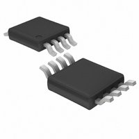
LTC1966CMS8#TRPBF Linear Technology, LTC1966CMS8#TRPBF Datasheet - Page 19

LTC1966CMS8#TRPBF
Manufacturer Part Number
LTC1966CMS8#TRPBF
Description
IC PREC RMS/DC CONV MCRPWR 8MSOP
Manufacturer
Linear Technology
Specifications of LTC1966CMS8#TRPBF
Current - Supply
155µA
Voltage - Supply
2.7 V ~ 5.5 V
Mounting Type
Surface Mount
Package / Case
8-MSOP, Micro8™, 8-uMAX, 8-uSOP,
Lead Free Status / RoHS Status
Lead free / RoHS Compliant
Available stocks
Company
Part Number
Manufacturer
Quantity
Price
Step Responses with a Post Filter
Both of the post filters, shown in Figures 13 and 14,
are optimized for additional filtering with clean step
responses. The 85kΩ output impedance of the LTC1966
working into a 1µF capacitor forms a 1st order LPF with
a –3dB frequency of ~1.8Hz. The two filters have 1µF at
the LTC1966 output for easy comparison with a 1µF only
case, and both have the same relative (Bessel-like) shape.
However, because of the topological differences of pole
placements between the various components within the
two filters, the net effective bandwidth for Figure 13 is
slightly higher (≈1.2 • 1.8 ≈ 2.1Hz) than with 1µF alone,
while the bandwidth for Figure 14 is somewhat lower
(≈0.7 • 1.8 ≈ 1.3Hz) than with 1µF alone. To adjust the
bandwidth of either of them, simply scale all the capacitors
by a common multiple, and leave the resistors unchanged.
The step responses of the LTC1966 with 1µF only and with
the two post filters are shown in Figure 15. This is the ris-
ing edge RMS output response to a 10Hz input starting
at t = 0. Although the falling edge response is the worst
case for settling, the rising edge illustrates the ripple that
these post filters are designed to address, so the rising
edge makes for a better intuitive comparison.
The initial rise of the LTC1966 will have enhanced slew rates
with DC and very low frequency inputs due to saturation
effects in the ∆S modulator. This is seen in Figure 15 in
two ways. First, the 1µF only output is seen to rise very
quickly in the first 40ms. The second way this effect shows
up is that the post filter outputs have a modest overshoot,
on the order of 3mV to 4mV, or 3% to 4%. This is only
applicaTions inForMaTion
FIGURE 13
FIGURE 14
1µF ONLY
RESPONSE
BURST
INPUT
STEP
Figure 15. Step Responses with 10Hz Burst
100ms/DIV
1966 F15
0
20mV/
DIV
0
200mV/
DIV
an issue with input frequency bursts at 50Hz or less, and
even with the overshoot, the settling to a given level of
accuracy improves due to the initial speedup.
As predicted by Figure 6, the DC error with 1µF is well
under 1mV and is not noticeable at this scale. However, as
predicted by Figure 8, the peak error with the ripple from a
10Hz input is much larger, in this case about 5mV. As can
be clearly seen, the post filters reduce this ripple. Even
the wider bandwidth of Figure 13’s filter is seen to cut the
ripple down substantially (to < 1mV) while the settling to
1% happens faster. With the narrower bandwidth of Figure
14’s filter, the step response is somewhat slower, but the
double frequency output ripple is just 180µV.
Figure 16 shows the step response of the same three cases
with a burst of 60Hz rather than 10Hz. With 60Hz, the ini-
tial portion of the step response is free of the boost seen
in Figure 15 and the two post filter responses have less
than 1% overshoot. The 1µF only case still has noticeable
120Hz ripple, but both filters have removed all detectable
ripple on this scale. This is to be expected; the first order
filter will reduce the ripple about 6:1 for a 6:1 change in
frequency, while the third order filters will reduce the
ripple about 6
Again, the two filter topologies have the same relative
shape, so the step response and ripple filtering trade-offs of
the two are the same, with the same performance of each
possible with the other by scaling it accordingly. Figures
17 and 18 show the peak error vs. frequency for a selec-
tion of capacitors for the two different filter topologies.
To keep the clean step response, scale all three capacitors
FIGURE 13
FIGURE 14
1µF ONLY
RESPONSE
BURST
INPUT
STEP
Figure 16. Step Responses with 60Hz Burst
3
:1 or 216:1 for a 6:1 change in frequency.
100ms/DIV
LTC1966
1966 F16
19
0
0
20mV/
DIV
200mV/
DIV
1966fb


