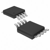
LTC1966CMS8#TRPBF Linear Technology, LTC1966CMS8#TRPBF Datasheet - Page 31

LTC1966CMS8#TRPBF
Manufacturer Part Number
LTC1966CMS8#TRPBF
Description
IC PREC RMS/DC CONV MCRPWR 8MSOP
Manufacturer
Linear Technology
Specifications of LTC1966CMS8#TRPBF
Current - Supply
155µA
Voltage - Supply
2.7 V ~ 5.5 V
Mounting Type
Surface Mount
Package / Case
8-MSOP, Micro8™, 8-uMAX, 8-uSOP,
Lead Free Status / RoHS Status
Lead free / RoHS Compliant
Available stocks
Company
Part Number
Manufacturer
Quantity
Price
applicaTions inForMaTion
The calculations of the error terms for a 200mV full-scale
case are:
DC, 2 Point
DC based calibration is preferable in many cases because a
DC voltage of known, good accuracy is easier to generate
than such an AC calibration voltage. The only down side
is that the LTC1966 input offset voltage plays a role. It is
therefore suggested that a DC based calibration scheme
check at least two points: ±full-scale. Applying the –full-
scale input can be done by physically inverting the voltage
or by applying the same +full-scale input to the opposite
LTC1966 input.
For an otherwise AC-coupled application, only the gain
term may be worth correcting for, but for DC-coupled ap-
plications, the input offset voltage can also be calculated
and corrected for.
The calculations of the error terms for a 200mV full-scale
case are:
Gain =
Input Offset =
Gain =
Output Offset =
Reading at 200mV + Reading at – 200mV
Reading at 200mV – Reading at 20mV
Reading at – 200mV – Reading at 200mV
Reading at 20mV
400mV
180mV
Gain
2 •Gain
– 20mV
Note: Calculation of and correction for input offset voltage
are the only way in which the two LTC1966 inputs (IN1,
IN2) are distinguishable from each other. The calculation
above assumes the standard definition of offset; that a
positive offset is the case of a positive voltage error inside
the device that must be corrected by applying a like nega-
tive voltage outside. The offset is referred to whichever
pin is driven positive for the +full-scale reading.
DC, 3 Point
One more point is needed with a DC calibration scheme
to determine output offset voltage: +10% of full scale.
The calculation of the input offset is the same as for the
2-point calibration above, while the gain and output offset
are calculated for a 200mV full-scale case as:
Gain =
Output Offset =
Reading at 200mV +Reading at – 200mV – 400mV • Gain
Reading at 200mV – Reading at 20mV
180mV
2
LTC1966
31
1966fb


