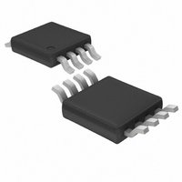
LTC1966CMS8#TRPBF Linear Technology, LTC1966CMS8#TRPBF Datasheet - Page 29

LTC1966CMS8#TRPBF
Manufacturer Part Number
LTC1966CMS8#TRPBF
Description
IC PREC RMS/DC CONV MCRPWR 8MSOP
Manufacturer
Linear Technology
Specifications of LTC1966CMS8#TRPBF
Current - Supply
155µA
Voltage - Supply
2.7 V ~ 5.5 V
Mounting Type
Surface Mount
Package / Case
8-MSOP, Micro8™, 8-uMAX, 8-uSOP,
Lead Free Status / RoHS Status
Lead free / RoHS Compliant
Available stocks
Company
Part Number
Manufacturer
Quantity
Price
As is shown in Figure 25b, where the LTC2420 is set to
continuously convert by grounding the CS pin. The gain
error will be less if CS is driven at a slower rate, however,
the rate should either be consistent or at a rate low enough
that the LTC1966 and its output capacitor have fully settled
by the beginning of each conversion, so that the loading
errors are consistent.
Note that in this circuit, the input current of the LTC2420
is being used to assure monotonicity. The LTC2420 Z
16.6MΩ is effectively connected to half the reference volt-
age, so when the LTC1966 has zero signal, 500mV/16.6MΩ
= 30nA is provided.
Alternatively, a 5V V
LTC1966 output span will only use 20% of the LTC2420’s
input voltage range. Furthermore, if the OUTRTN remains
grounded, the injected current with zero signal will be
150nA, resulting in 5× the offset error and nonlinearity
shown in Figure 22.
In both of the circuits of Figure 25, a guard ring only has to
encircle three terminals, the LTC1966 output, the top of the
averaging capacitor, and the ADC input. Figure 26 shows
the top copper patterns for example PCB layouts of each.
The low power consumption of the LTC1966 makes it well
suited for battery powered applications, and its slow output
(DC) makes it an ideal candidate for a micropower ADC.
applicaTions inForMaTion
Figure 26a. PCB Layout of Figure 25a with Guard Ring
LTC1966
MS8
C
AVE
REF
1µf
can be used, but in this case the
ICL7106
MQFP
1966 F26a
IN
of
Figure 10 in Application Note 75, for instance, details a
10-bit ADC with a 35ms conversion time that uses just
29µA of supply current. Such an ADC may also be of use
within a 4mA to 20mA loop.
Other types of ADCs sample the input signal once and
perform a conversion on that one sample. With these ADCs
(Nyquist ADCs), a post filter will be needed in most cases
to reduce the peak error with low input frequencies. The
DC accurate filter of Figure 14 is attractive from an error
standpoint, but it increases the impedance at the ADC
input. In most cases, the buffered post filter of Figure 13
will be more appropriate for use with Nyquist analog-to-
digital converters.
SYSTEM CALIBRATION
The LTC1966 static accuracy can be improved with end
system calibration. Traditionally, calibration has been
done at the factory, or at a service depot only, typically
using manually adjusted potentiometers. Increasingly,
systems are being designed for electronic calibration
where the accuracy corrections are implemented in digital
code wherever possible, and with calibration DACs where
necessary. Additionally, many systems are now designed
for self calibration, in which the calibration occurs inside
the machine, automatically without user intervention.
Figure 26b. PCB Layout of Figure 25b with Guard Ring
LTC1966
MS8
C
AVE
1µf
LTC2420
LTC1966
SO8
1966 F26b
29
1966fb


