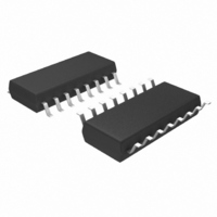
FAN7392MX Fairchild Semiconductor, FAN7392MX Datasheet - Page 14

FAN7392MX
Manufacturer Part Number
FAN7392MX
Description
IC GATE DVR MONO HI/LO 16SOP
Manufacturer
Fairchild Semiconductor
Type
High Side/Low Sider
Datasheet
1.FAN7392MX.pdf
(18 pages)
Specifications of FAN7392MX
Configuration
Half Bridge
Input Type
Non-Inverting
Delay Time
130ns
Current - Peak
3A
Number Of Configurations
1
Number Of Outputs
2
High Side Voltage - Max (bootstrap)
600V
Voltage - Supply
10 V ~ 20 V
Operating Temperature
-40°C ~ 125°C
Mounting Type
Surface Mount
Package / Case
16-SOIC (0.300", 7.5mm Width)
Product
H-Bridge Drivers
Rise Time
50 ns
Fall Time
45 ns
Supply Voltage (min)
3.3 V
Supply Current
0.43 mA
Maximum Power Dissipation
1300 mW
Maximum Operating Temperature
+ 125 C
Mounting Style
SMD/SMT
Bridge Type
Full Bridge, Half Bridge
Minimum Operating Temperature
- 40 C
Number Of Drivers
2
Lead Free Status / RoHS Status
Lead free / RoHS Compliant
Other names
FAN7392MXTR
Available stocks
Company
Part Number
Manufacturer
Quantity
Price
Company:
Part Number:
FAN7392MX
Manufacturer:
FSC
Quantity:
772
Part Number:
FAN7392MX
Manufacturer:
FAIRCHILD/仙童
Quantity:
20 000
FAN7392 Rev. 1.0.3
© 2009 Fairchild Semiconductor Corporation
Application Information
Negative V
The bootstrap circuit has the advantage of being simple
and low cost, but has some limitations. The biggest diffi-
culty with this circuit is the negative voltage present at
the emitter of the high-side switching device when high-
side switch is turned-off in half-bridge application.
If the high-side switch, Q1, turns-off while the load cur-
rent is flowing to an inductive load, a current commuta-
tion occurs from high-side switch, Q1, to the diode, D2,
in parallel with the low-side switch of the same inverter
leg. Then the negative voltage present at the emitter of
the high-side switching device, just before the freewheel-
ing diode, D2, starts clamping, causes load current to
suddenly flow to the low-side freewheeling diode, D2, as
shown in Figure 34.
This negative voltage can be trouble for the gate driver’s
output stage, there is the possibility to develop an over-
voltage condition of the bootstrap capacitor, input signal
missing and latch-up problems because it directly affects
the source V
35. This undershoot voltage is called “negative V
sient”.
Figure 35. V
Figure 34. Half-Bridge Application Circuits
GND
V
Q1
GND
S
S
S
DC+ Bus
pin of the gate driver, as shown in Figure
Transient
S
Waveforms During Q1 Turn-Off
Q1
V
Q2
S
D1
D2
i
i
LOAD
freewheeling
Load
Freewheeling
S
tran-
14
Figure 36 and Figure 37 show the commutation of the
load current between high-side switch, Q1, and low-side
freewheelling diode, D3, in same inverter leg. The para-
sitic inductances in the inverter circuit from the die wire
bonding to the PCB tracks are jumped together in L
L
low-side switch, Q4, are turned on, the V
below DC+ voltage by the voltage drops associated with
the power switch and the parasitic inductances of the cir-
cuit due to load current is flows from Q1 and Q4, as
shown in Figure 36. When the high-side switch, Q1, is
turned off and Q4, remained turned on, the load current
to flows the low-side freewheeling diode, D3, due to the
inductive load connected to VS1 as shown in Figure 37.
The current flows from ground (which is connected to the
COM pin of the gate driver) to the load and the negative
voltage present at the emitter of the high-side switching
device.
In this case, the COM pin of the gate driver is at a higher
potential than the V
ated with freewheeling diode, D3, and parasitic ele-
ments, L
E
for each IGBT. When the high-side switch, Q1, and
Figure 37. Q1 Turn-Off and D3 Conducting
C3
and L
Figure 36. Q1 and Q4 Turn-On
DC+ Bus
DC+ Bus
E3
S
.
L
Q1
L
V
Q3
L
L
Q1
V
Q3
L
L
L
L
C1
E1
S1
C3
pin due to the voltage drops associ-
E3
C1
E1
S1
C3
E3
V
V
V
V
LC1
LE1
D1
D3
LC3
LE3
D1
D3
i
i
LOAD
freewheeling
i
i
LOAD
freewheeling
Load
Load
www.fairchildsemi.com
D2
D4
D2
D4
S1
V
V
V
V
LC4
LE4
LC4
LE4
node is
L
L
V
L
L
Q2
Q4
L
L
V
L
L
C2
Q2
Q4
E2
S2
C4
E4
C2
E2
S2
C4
E4
C
and


