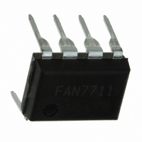
FAN7711N Fairchild Semiconductor, FAN7711N Datasheet - Page 11

FAN7711N
Manufacturer Part Number
FAN7711N
Description
IC BALLAST CONTROL HV 8-DIP
Manufacturer
Fairchild Semiconductor
Type
Ballast Controllerr
Specifications of FAN7711N
Frequency
48.7 ~ 57.3 kHz
Current - Supply
3.2mA
Current - Output
650mA
Operating Temperature
-25°C ~ 125°C
Package / Case
8-DIP (0.300", 7.62mm)
Switching Frequency
95 KHz
Operating Temperature Range
- 25 C to + 125 C
Mounting Style
Through Hole
Lead Free Status / RoHS Status
Lead free / RoHS Compliant
Voltage - Supply
-
Lead Free Status / Rohs Status
Lead free / RoHS Compliant
Available stocks
Company
Part Number
Manufacturer
Quantity
Price
Company:
Part Number:
FAN7711N
Manufacturer:
FSC
Quantity:
15 000
FAN7711 Rev. 1.0.3
© 2007 Fairchild Semiconductor Corporation
Assuming that C
respectively; the power dissipation reaches about 2.4W
and the temperature of FAN7711 is increased rapidly. If
no protection is provided, the IC can be damaged by the
thermal attack. Note that hard-switching condition during
the capacitive-load drive causes lots of EMI.
Figure 24 illustrates the waveforms during the open-
lamp condition. In this condition, the charging and
discharging current of C
FAN7711 and considered hard-switching condition. The
FAN7711 tries to meet ZVS condition by decreasing
CPH voltage to increase dead time. If ZVS fails and CPH
goes below 2V, even though the dead time reaches its
maximum value, FAN7711 shuts off the IC to protect
against damage. To restart FAN7711, V
below V
remembers the status of the IC.
FAN7711 Rev. 1.00
V
V
Figure 23. Current Flow When the Lamp is Open
Figure 24. CPH Voltage Variation in Open-Lamp
DDTH(ST+)
DDTH(ST-)
C
VDD
CPH
OUT
V
6V
5V
3V
2V
RT
DD
0V
(Filament warm-up)
Preheating period
CPH
DDTH(ST-)
CPH
GND
V
RT
DD
FAN7711
Oscillator
Dead-time
controller
P
, V
to reset an internal latch circuit, which
DB
DC
Active ZVS activated
High-side
Low-side
driver
driver
, and f are 1nF, 311V, and 50kHz,
Condition
Ignition period
P
Charge Pump
Dp1
HO
LO
V
V
Running mode
Active ZVS mode
is directly determined by
B
S
C
CP
Automatic
Shutdown
Shutdown
Release Restart
Dp2
C
V
Shutdown
B
DC
mode
LCC resonant tank
equivalent lamp impedance
L
FAN7711 Rev. 1.00
DD
C
S
R
L
must be
Filament Open
time
time
C
time
P
11
5. Power Supply
When V
little current, I
the V
Figure 25). Once UVLO is released, the current
consumption is increased and whole circuits are
operated, which requires additional power supply for
stable operation. The supply must deliver at least several
mA. A charge pump circuit is a cost-effective method to
create an additional power supply and allows C
used to reduce the EMI.
As presented in Figure 25, when V
current and C
slope of dv/dt. The rising edge of V
time, the current that flows through C
This current flows along the path (1). It charges C
which is a bypass capacitor to reduce the noise on the
supply rail. If C
of the internal shunt regulator, the shunt regulator is
turned on and regulates V
When V
discharged through Dp2, shown as path (2) in Figure 26.
These charging/discharging operations are continued
until FAN7711 is halted by shutdown operation. The
charging current, I, must be large enough to supply the
operating current of FAN7711.
The supply for the high-side gate driver is provided by
the boot-strap technique, as illustrated in Figure 26.
When the low-side MOSFET connected between V
GND pins is turned on, the charging current for V
through D
C
operates normally.
B
FAN7711 Rev. 1.00
. Therefore C
Figure 25. Local Power Supply for V
+
C
DD
R
VDD
start
DD
pin using a resistor with high resistance (R
S
B
GND
CPH
V
RT
is changing from high to low state, C
. Every low V
DD
is lower than V
ST
(1)
CP
VDD
, making it possible to supply current to
B
FAN7711
Charge Pump Circuit
regulator
voltage builds up only when FAN7711
create an output transition with the
Shunt
DB
is charged over the threshold voltage
I
≅
S
C
gives the chance to charge the
DD
CP
DDTH(ST+)
Charge Pump
×
HO
LO
with the trigger voltage.
V
V
Dp1
B
S
Ccp
dv
dt
Dp2
S
C
S
V
B
charges C
DC
is high, the inductor
CP
, it consumes very
(2)
is:
dv/dt
LCC resonant tank
equivalent lamp impedance
DD
L
www.fairchildsemi.com
C
Using a
R
S
CP
L
Filament Open
. At that
P
(EQ 7)
B
start
S
to be
CP
flows
C
VDD
P
and
in
is
,


