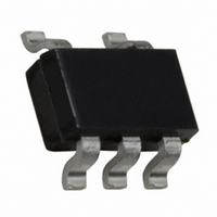
FAN5331SX Fairchild Semiconductor, FAN5331SX Datasheet - Page 6

FAN5331SX
Manufacturer Part Number
FAN5331SX
Description
IC LED DRVR WHITE BCKLGT SOT23-5
Manufacturer
Fairchild Semiconductor
Type
Backlight, White LED (Serial Interface)r
Datasheet
1.FAN5331SX.pdf
(10 pages)
Specifications of FAN5331SX
Topology
PWM, Step-Up (Boost)
Number Of Outputs
1
Internal Driver
Yes
Type - Primary
General Purpose
Frequency
1.15MHz ~ 1.85MHz
Voltage - Supply
2.7 V ~ 5.5 V
Voltage - Output
20V
Mounting Type
Surface Mount
Package / Case
SOT-23-5, SC-74A, SOT-25
Operating Temperature
-40°C ~ 85°C
Current - Output / Channel
50mA
Internal Switch(s)
Yes
Efficiency
88%
Operating Supply Voltage (typ)
3.3/5V
Operating Temperature (min)
-40C
Operating Temperature (max)
85C
Operating Temperature Classification
Industrial
Package Type
SOT-23
Pin Count
5
Mounting
Surface Mount
Operating Supply Voltage (min)
2.7V
Operating Supply Voltage (max)
5.5V
Low Level Output Current
50 mA
Operating Supply Voltage
2.7 V to 5.5 V
Maximum Supply Current
3 mA
Maximum Operating Temperature
+ 85 C
Mounting Style
SMD/SMT
Minimum Operating Temperature
- 40 C
Primary Input Voltage
5.5V
No. Of Outputs
1
Output Voltage
20V
No. Of Pins
5
Operating Temperature Range
-40°C To +85°C
Peak Reflow Compatible (260 C)
Yes
Leaded Process Compatible
Yes
Rohs Compliant
Yes
Dc
N/A
Lead Free Status / RoHS Status
Lead free / RoHS Compliant
Other names
FAN5331SXTR
FAN5331SX_NL
FAN5331SX_NLTR
FAN5331SX_NLTR
FAN5331SX_NL
FAN5331SX_NLTR
FAN5331SX_NLTR
Available stocks
Company
Part Number
Manufacturer
Quantity
Price
Company:
Part Number:
FAN5331SX
Manufacturer:
FSC
Quantity:
3 000
Part Number:
FAN5331SX
Manufacturer:
FAIRCHILD/仙童
Quantity:
20 000
Part Number:
FAN5331SX_NL
Manufacturer:
FAIRCHILD/仙童
Quantity:
20 000
FAN5331 Rev. 1.0.1
Block Diagram
Circuit Description
The FAN5331 is a pulse-width modulated (PWM) current-mode
boost converter. The FAN5331 improves the performance of bat-
tery powered equipment by significantly minimizing the spectral
distribution of noise at the input caused by the switching action of
the regulator. In order to facilitate effective noise filtering, the
switching frequency was chosen to be high, 1.6MHz. An internal
soft start circuitry minimizes in-rush currents. The timing of the soft
start circuit was chosen to reach 95% of the nominal output voltage
within maximum 5mS following an enable command when V
2.7V, V
The device architecture is that of a current mode controller with
an internal sense resistor connected in series with the N-chan-
nel switch. The voltage at the feedback pin tracks the output
voltage at the cathode of the external Schottky diode (shown in
the test circuit). The error amplifier amplifies the difference
between the feedback voltage and the internal bandgap refer-
ence. The amplified error voltage serves as a reference voltage
to the PWM comparator. The inverting input of the PWM com-
parator consists of the sum of two components: the amplified
control signal received from the 50m
and the ramp generator voltage derived from the oscillator. The
oscillator sets the latch, and the latch turns on the FET switch.
Under normal operating conditions, the PWM comparator resets
the latch and turns off the FET, thus terminating the pulse.
Since the comparator input contains information about the out-
put voltage and the control loop is arranged to form a negative
feedback loop, the value of the peak inductor current will be
adjusted to maintain regulation.
Every time the latch is reset, the FET is turned off and the cur-
rent flow through the switch is terminated. The latch can be
OUT
= 15V, I
LOAD
FB
= 35mA and C
3
Shutdown
Circuitry
SHDN
4
OUT (EFFECTIVE)
Generator
1.15 x V
-
Error
Amp
+
Oscillator
current sense resistor
Ramp
Reference
FB
REF
Shutdown
Thermal
Figure 4. Block Diagram
S
+
-
= 3.2 F.
Over
Voltage
Comp
Current Limit
Comparator
Comp
+
Soft-Start
V
-
IN
5
IN
=
6
-
reset by other events as well. Over-current condition is moni-
tored by the current limit comparator which resets the latch and
turns off the switch instantaneously within each clock cycle.
Over-Voltage Protection
The voltage on the feedback pin is sensed by an OVP Compar-
ator. When the feedback voltage is 15% higher than the nominal
voltage, the OVP Comparator stops switching of the power tran-
sistor, thus preventing the output voltage from going higher.
Applications Information
Setting the Output Voltage
The internal reference is 1.23V (Typical). The output voltage is
divided by a resistor divider, R1 and R2 to the FB pin. The out-
put voltage is given by
According to this equation, and assuming desired output volt-
age of 15V, good choices for the feedback resistors are,
R
Inductor Selection
The inductor parameters directly related to device performances
are saturation current and dc resistance. The FAN5331 oper-
ates with a typical inductor value of 10µH. The lower the dc
resistance, the higher the efficiency. Usually a trade-off between
inductor size, cost and overall efficiency is needed to make the
optimum choice.
+
1
=150k and R
R
R
R
S
Q
2
=13.4k .
V
Driver
OUT
=
Amp
V
REF
+
-
n
GND
SW
2
1
1
0.05
+
R
------ -
R
1
2
www.fairchildsemi.com


