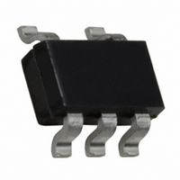
FAN5331SX Fairchild Semiconductor, FAN5331SX Datasheet - Page 2

FAN5331SX
Manufacturer Part Number
FAN5331SX
Description
IC LED DRVR WHITE BCKLGT SOT23-5
Manufacturer
Fairchild Semiconductor
Type
Backlight, White LED (Serial Interface)r
Datasheet
1.FAN5331SX.pdf
(10 pages)
Specifications of FAN5331SX
Topology
PWM, Step-Up (Boost)
Number Of Outputs
1
Internal Driver
Yes
Type - Primary
General Purpose
Frequency
1.15MHz ~ 1.85MHz
Voltage - Supply
2.7 V ~ 5.5 V
Voltage - Output
20V
Mounting Type
Surface Mount
Package / Case
SOT-23-5, SC-74A, SOT-25
Operating Temperature
-40°C ~ 85°C
Current - Output / Channel
50mA
Internal Switch(s)
Yes
Efficiency
88%
Operating Supply Voltage (typ)
3.3/5V
Operating Temperature (min)
-40C
Operating Temperature (max)
85C
Operating Temperature Classification
Industrial
Package Type
SOT-23
Pin Count
5
Mounting
Surface Mount
Operating Supply Voltage (min)
2.7V
Operating Supply Voltage (max)
5.5V
Low Level Output Current
50 mA
Operating Supply Voltage
2.7 V to 5.5 V
Maximum Supply Current
3 mA
Maximum Operating Temperature
+ 85 C
Mounting Style
SMD/SMT
Minimum Operating Temperature
- 40 C
Primary Input Voltage
5.5V
No. Of Outputs
1
Output Voltage
20V
No. Of Pins
5
Operating Temperature Range
-40°C To +85°C
Peak Reflow Compatible (260 C)
Yes
Leaded Process Compatible
Yes
Rohs Compliant
Yes
Dc
N/A
Lead Free Status / RoHS Status
Lead free / RoHS Compliant
Other names
FAN5331SXTR
FAN5331SX_NL
FAN5331SX_NLTR
FAN5331SX_NLTR
FAN5331SX_NL
FAN5331SX_NLTR
FAN5331SX_NLTR
Available stocks
Company
Part Number
Manufacturer
Quantity
Price
Company:
Part Number:
FAN5331SX
Manufacturer:
FSC
Quantity:
3 000
Part Number:
FAN5331SX
Manufacturer:
FAIRCHILD/仙童
Quantity:
20 000
Part Number:
FAN5331SX_NL
Manufacturer:
FAIRCHILD/仙童
Quantity:
20 000
FAN5331 Rev. 1.0.1
Pin Assignment
Pin Description
Absolute Maximum Ratings (
Recommended Operating Conditions
Notes:
1. Stresses above those listed under “Absolute Maximum Ratings” may cause permanent damage to the device. This
2. Using EIA/JESD22A114B (Human Body Model) and EIA/JESD22C101-A (Charge Device Model).
3. This load capacitance value is required for the loop stability. Tolerance, temperature variation, and voltage
V
FB, SHDN to GND
SW to GND
Lead Soldering Temperature (10 seconds)
Junction Temperature
Storage Temperature
Thermal Resistance (
Electrostatic Discharge Protection (ESD) Level (Note 2)
Input Voltage
Output Voltage
Operating Ambient Temperature
Output Capacitance (Note 3)
IN
Pin No.
is a stress rating only and functional operation of the device at these or any other conditions above those indicated
in the operational section of this specification is not implied. Exposure to absolute maximum rating conditions for
extended periods may affect device reliability. Absolute maximum ratings apply individually only, not in combination.
dependency of the capacitance must be considered. Typically a 4.7µF ceramic capacitor is required to achieve
specified value at V
to GND
1
2
3
4
5
Pin Name
SHDN
JA
GND
SW
V
FB
)
OUT
IN
= 15V.
Parameter
Switching node.
Analog and power ground.
Feedback node that connects to an external voltage divider.
Shutdown control pin. Logic HIGH enables, logic LOW disables the device.
Input voltage.
Parameter
Note1)
Figure 2. Pin Assignment
GND
SW
FB
5-Lead SOT-23
Top View
2
SHDN
V
IN
Pin Description
HBM
CDM
Min
2.7
V
-40
1.6
IN
Typ
Min
-0.3
-0.3
-55
2.5
25
1
V
IN
Max
Max
300
150
150
265
5.5
6.0
20
85
23
+ 0.3
www.fairchildsemi.com
Unit
Unit
°C/W
°C
µF
°C
°C
°C
kV
V
V
V
V
V


