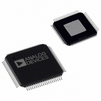
AD8384ASVZ Analog Devices Inc, AD8384ASVZ Datasheet - Page 9

AD8384ASVZ
Manufacturer Part Number
AD8384ASVZ
Description
IC DRIVER LCD 6CH 10BIT 80-TQFP
Manufacturer
Analog Devices Inc
Series
DecDriver™r
Datasheet
1.AD8384ASVZ.pdf
(24 pages)
Specifications of AD8384ASVZ
Display Type
LCD
Interface
3-Wire Serial
Current - Supply
40mA
Voltage - Supply
9 V ~ 18 V
Operating Temperature
0°C ~ 85°C
Mounting Type
Surface Mount
Package / Case
80-TQFP Exposed Pad, 80-eTQFP, 80-HTQFP, 80-VQFP
Lead Free Status / RoHS Status
Lead free / RoHS Compliant
Configuration
-
Digits Or Characters
-
Available stocks
Company
Part Number
Manufacturer
Quantity
Price
Company:
Part Number:
AD8384ASVZ
Manufacturer:
Analog Devices Inc
Quantity:
10 000
PIN CONFIGURATION AND FUNCTION DESCRIPTIONS
Table 7. Pin Function Descriptions
Pin Name
DB(0:9)
CLK
STSQ
R/L
E/O
XFR
VID0–VID5
V1, V2
VRH, VRL
BYP
Clock
Data Transfer
Analog Outputs
Reference Voltages
Full-Scale References
Function
Data Input
Start Sequence
Right/Left Select
Even/Odd Select
Bypass
NC =
NO CONNECT
AGNDS
AVCCS
DIRXIN
DIRYIN
DGND
TSTM
STSQ
SVRH
VAO1
VAO2
SVRL
CLK
SEN
XFR
SCL
E/O
INV
SDI
R/L
NC
10
11
12
13
14
15
16
17
18
19
20
Figure 3. 80-Lead 12 mm × 12 mm TQFP E-Pad Pin Configuration
1
2
3
4
5
6
7
8
9
80 79 78 77 76
21 22 23 24 25 26 27 28 29 30 31 32 33 34 35 36 37 38 39 40
PIN 1
IDENTIFIER
Description
10-Bit Data Input. MSB = DB(9).
Clock Input.
The state of STSQ is detected on the active edge of CLK. A new data loading sequence
begins on the next active edge of CLK after STSQ is detected HIGH.
The active CLK edge is the rising edge when E/O is held HIGH. It is the falling edge when
E/O is held LOW.
A new data loading sequence begins on the left, with Channel 0, when this input is LOW,
and on the right, with Channel 5, when this input is HIGH.
The active CLK edge is the rising edge when this input is held HIGH. It is the falling edge
when this input is held LOW. Data is loaded sequentially on the rising edges of CLK when
this input is HIGH and on the falling edges when this input is LOW.
XFR is detected and a data transfer is initiated on a rising CLK edge when this input is held
HIGH. Data is transferred to the video outputs on the next rising CLK edge after XFR is
detected.
These pins are directly connected to the analog inputs of the LCD panel.
The voltage applied between V1 and AGND sets the white video level during INV = LOW.
The voltage applied between V2 and AGND sets the white video level during INV = HIGH.
Twice the voltage applied between these pins sets the full-scale video output voltage.
A 0.1µ F capacitor connected between this pin and AGND ensures optimum settling time.
75 74 73 72
Rev. 0 | Page 9 of 24
(Not to Scale)
TOP VIEW
AD8384
71 70 69 68 67 66 65
64 63 62 61
60
59
58
57
56
55
54
53
52
51
50
49
48
47
46
45
44
43
42
41
AGND0
VID0
AVCC0,1
VID1
AGND1,2
VID2
AVCC2,3
VID3
AGND3,4
VID4
AVCC4,5
VID5
AGND5
CLXN
CLX
ENBX4
ENBX3
ENBX2
ENBX1
DX
AD8384


