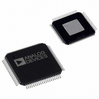
AD8384ASVZ Analog Devices Inc, AD8384ASVZ Datasheet - Page 10

AD8384ASVZ
Manufacturer Part Number
AD8384ASVZ
Description
IC DRIVER LCD 6CH 10BIT 80-TQFP
Manufacturer
Analog Devices Inc
Series
DecDriver™r
Datasheet
1.AD8384ASVZ.pdf
(24 pages)
Specifications of AD8384ASVZ
Display Type
LCD
Interface
3-Wire Serial
Current - Supply
40mA
Voltage - Supply
9 V ~ 18 V
Operating Temperature
0°C ~ 85°C
Mounting Type
Surface Mount
Package / Case
80-TQFP Exposed Pad, 80-eTQFP, 80-HTQFP, 80-VQFP
Lead Free Status / RoHS Status
Lead free / RoHS Compliant
Configuration
-
Digits Or Characters
-
Available stocks
Company
Part Number
Manufacturer
Quantity
Price
Company:
Part Number:
AD8384ASVZ
Manufacturer:
Analog Devices Inc
Quantity:
10 000
AD8384
Pin Name
INV
DVCC
DGND
AVCCx
AGNDx
SVRH, SVRL
SCL
SDI
SEN
VAO1, VAO2
TSTM
MONITI
MONITO
DYIN, DIRYIN,
DIRXIN, DXIN,
NRGIN, ENBX(1–4)IN
DX, DY, DIRX, DIRY,
NRG, ENBX(1-4)
CLXIN, CLYIN
CLX, CLXN, CLY,
CLYN,
Function
Invert
Digital Power Supply
Digital Ground
Analog Power
Supplies
Analog Ground
Serial DAC Reference
Voltages
Serial Data Clock
Data Input
Serial DAC Enable
Serial DAC Voltage
Output
Test Mode
Monitor Input
Monitor Output
Inverting Level
Shifter Inputs
Inverting Level
Shifter Outputs
Complementary
Level Shifter Inputs
Complementary
Level Shifter Outputs
Description
When this input is HIGH, the VIDx output voltages are above V2. When INV is LOW, the VIDx
output voltages are below V1.
The state of INV is latched on the first rising CLK edge, after XFR is detected. The VIDx
outputs change on the rising CLK edge after the next XFR is detected.
Digital Power Supply.
This pin is normally connected to the digital ground plane.
Analog Power Supplies.
Analog Supply Returns.
Reference Voltages for the Output Amplifiers of the Control DACs.
Serial Data Clock.
While the SEN input is LOW, one 12-bit serial word is loaded into the serial DAC on the
rising edges of SCL. The first bit selects the output, the next three bits are unused, and the
subsequent eight bits are the data used in the DAC.
A falling edge of this input initiates a loading cycle. While this input is held LOW, the serial
DAC is enabled and data is loaded on every rising edge of SCL. The selected output is
updated on the rising edge of this input. While this input is held HIGH, the control DAC is
disabled.
These output voltages are updated on the rising edge of the SEN input.
When this input is LOW, the output mode is determined by the function programmed into
the serial interface.
While this input is held HIGH, the output mode is forced to NORMAL, regardless of function
programmed into the serial interface.
Logic Input of the Level Shifting Inverting Edge Detector.
Output of the Level Shifting Inverting Edge Detector.
Logic Input of the Inverting Level Shifters.
While the corresponding input voltage of these level shifters is below the threshold
voltage, the output voltage at these pins is at VOH.
While the corresponding input voltage of these level shifters is above the threshold
voltage, the output voltage at these pins is at VOL.
Logic Input of the Complementary Level Shifters.
While the corresponding input voltage of these level shifters is below the threshold
voltage, the voltage at the noninverting output pins is at VOH and the voltage at the
inverting outputs is at VOL.
While the corresponding input voltage of these level shifters is above the threshold
voltage, the voltage at the noninverting output pins is at VOL and the voltage at the
inverting outputs is at VOH.
Rev. 0 | Page 10 of 24


